
GE VMIVME-3126 High Resolution Isolated Analog to Digital Converter Board
GE VMIVME-3126 High Resolution Isolated Analog to Digital Converter Board
Product Overview
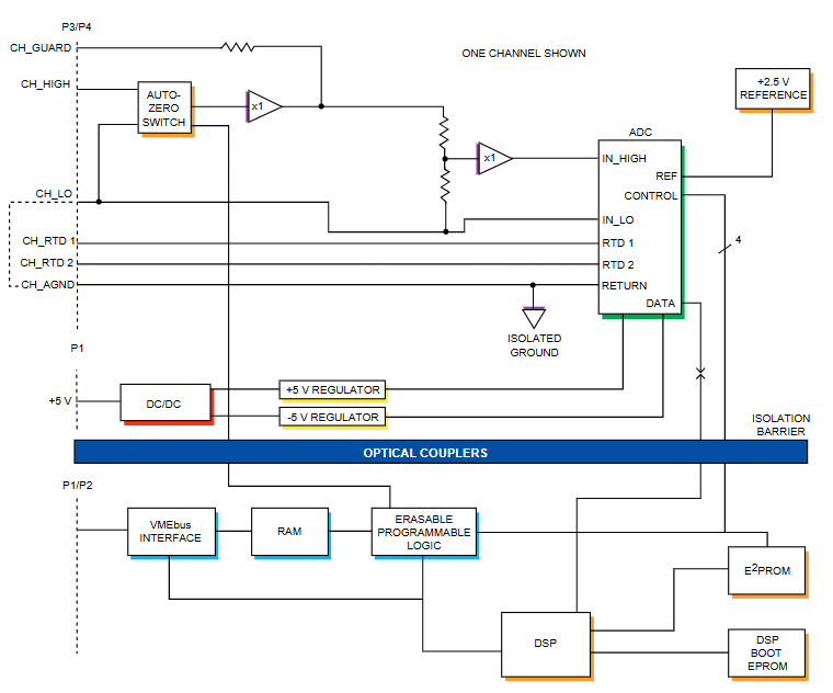
VMIVME-3126 is an 8-channel or 16 channel high-resolution fully isolated analog-to-digital converter (ADC) board that can accept 2-wire isolated signals ranging from 50 mV to 10 V as input, providing isolation between channels and between channels and VMEbus. Each input is sampled and digitized by a dedicated 24 bit analog-to-digital converter, which automatically scans all inputs after on-board self-test is completed upon power on. Its accuracy is optimized through internal gain and offset correction, which are applied by a digital signal processor (DSP) in real-time mode and determined in calibration mode.
Core functions and parameters
Key Features
8 or 16 isolated input channels with source protection, 16 bit data.
The isolation voltage between channels and between channels and VMEbus is 1500 VDC (1000 VAC).
Each channel is equipped with a dedicated digitizer with an input range of ± 50 mV to ± 10 V, which can be selected by software according to the channel.
Software controlled bandwidth, 0.05 to 26 Hz (implemented through an internal DSP with a 6th order low-pass filter).
Real time offset and gain correction based on DSP, with E ² PROM storage of calibration coefficients supported by DSP (without fine adjustment potentiometer).
The conversion rate per channel is 100 SPS (samples per second).
Software controlled RTD excitation (200 mA/400 mA per channel), software controlled open circuit sensor detection.
Supported by VMIC's I/O controller, optional current termination resistors and optional increase in input range are available.
Application field
Including power plant monitoring, machine monitoring, data acquisition, as well as applications related to RTDs, strain gauges, and thermocouples.
Features
VMEbus access and compatibility: The response to address modifiers can be selected through jumpers, including A24 or A16 address space, monitoring or user permissions (or both), D16/D8 (EO) DTB slave, with a 6U external specification.
Board address: The VMEbus base address is configured by jumper fields, and each address A23 to A8 has a jumper, so the address space occupied by the board is 256 bytes.
Operation Mode
Sampling mode: After successful onboard self-test, all inputs are sampled simultaneously when powered on.
Calibration mode: Enter calibration mode by setting the bits in the board and status register (BSR). Each channel is calibrated by the DSP using up to seven external calibration voltage inputs. The gain and offset coefficients are stored in the DSP for real-time calibration. Users can set another bit in the BSR to write the coefficients to the E ² PROM or input their own gain and offset coefficients.
Configuration mode: Enter configuration mode by setting the bit in BSR, and each channel can be individually configured with range, filter frequency, data output format, and input type (normal, RTD excitation, open circuit sensor detection).
Automatic zeroing mode: Enter the automatic zeroing mode by setting the bit in BSR. In this mode, each input is disconnected from the field through an electronic switch, connected to a ground reference, digitized, and compared with the ideal ground reading. Adjust the offset coefficient to eliminate this difference. This technology can compensate for temperature changes without calibration operations.
Self check: After the system or software is reset, it automatically runs a self check to test the onboard RAM and each ADC. The status register indicates the success or failure status of these components.
Front panel indicator: The program controlled front panel LED lights up red during startup, calibration, and channel reconfiguration, and turns off after successfully completing the above modes.
Board Identification: The Board Identification Register (BIR) contains the VMIVME-3126 identification code.
Input characteristics
Number of input channels: 8 or 16 isolated 2-wire channels, each with an active protection pin.
Isolation voltage: 1500 VDC and 1000 VAC between channels and between channels and VME.

Input range (software control)
Bipolar: ± 50 mV, ± 100 mV, ± 500 mV, ± 1 V, ± 5 V, ± 10 V
Monopolar: 0 to 50 mV, 0 to 100 mV, 0 to 500 mV, 0 to 1 V, 0 to 5 V, 0 to 10 V
Input filter: 0.05 to 26 Hz low-pass, 6th order, filter cut-off frequency controlled by software, filtering executed by DSP software, approximate Bessel response.
Accuracy: The accuracy of the full-scale range varies in different ranges, such as ± 10 V, ± 5 V, 0-10 V, 0-5 V for 0.0030% full-scale, ± 1 V for 0.0076% full-scale, etc. (applicable after calibration of the selected input voltage range).
Stability: The temperature drift is ± V/° C, and the offset error caused by temperature can be eliminated by automatic zeroing.
Input noise: The typical and maximum noise varies under different filter settings and ranges, with noise units in μ V RMS.
Bandwidth of each input: DC to Fc, Fc is 0.05 to 26 Hz (default cutoff frequency is 26 Hz).
Input impedance: minimum, powered on (not applicable to boards equipped with current input options).
Channel crosstalk: The maximum is -150 dB at 1 kHz and Fc=1 Hz.
Isolation mode suppression: 160 dB at 60 Hz and Fc=1 Hz.
Overvoltage protection: ± 25 V wire to wire.
RTD excitation (software control per channel): typical 20 PPM/° C, maximum 20%.
Open circuit sensor detection (controlled by software for each channel): It functions normally in all ranges below ± 1 V (0-1 V).
Channel protection: Active output with unity gain and 1 k Ω source impedance.
Current terminal resistance: see the available options section.
Transmission characteristics
Transfer function: E IN=E LO+[E fsr × 65536N ADC], where E IN is the channel input voltage, E LO
For the lower limit of the input range, E fsr is the full-scale input range, and N ADC is the output code.
Resolution: 16 bits.
Input sampling: All inputs are sampled simultaneously.
Integral nonlinearity: maximum ± 0.005% compared to the optimal straight line.
Channel sampling rate: 100 SPS per channel, total 1600 SPS.
Data encoding: Software programmable, binary complement or straight/offset binary.
Data buffer memory
Buffer size: 16 consecutive 16 bit data words.
Access time: 400 ns from DS to DTACK.
VMEbus access: D8 or D16.

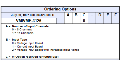
Available options (see ordering options)
Number of input channels: 8 or 16 2-wire channels.
Current terminal resistor: a resistor placed at both ends of the input, with a maximum continuous input current of 25 mA (calibrated input specified in current units rather than voltage units).
Increase input range: The input structure can handle an input range of up to ± 200 VDC.
Physical/Environmental Characteristics
Temperature range: working (standard VME slot) 0 to+65 ° C, storage -40 to+85 ° C.
Humidity: 10 to 80% relative humidity, no condensation.
Altitude: Working up to 10000 feet (3048 meters).
Cooling: forced air convection (standard VME slot).
Size: Dual height European card (6U) board, 160 x 233.35mm.
Weight: Maximum 700 g.
Input connectors: Two 64 pin DIN connectors.
Connector data
Recommended style for connecting components P3 and P4 I/O connectors
64 pin, compatible connector (96 pin discrete) AMP 925486-1*
Discrete line, female pressure contact point (64 pin discrete) AMP 530151-6**
(64 pin connector) connector housing Harting 09 02 064 0501
Note: * The middle row is not connected; **AMP crimping tool part number 90301-2.
Power requirements
+5 VDC (± 5%), maximum 2.8 A.
Mean Time Between Failures (MTBF)
97850 hours (217F).
- OMRON
- ABB
- General Electric
- EMERSON
- Honeywell
- HIMA
- ALSTOM
- Rolls-Royce
- MOTOROLA
- Rockwell
- Siemens
- Woodward
- YOKOGAWA
- FOXBORO
- KOLLMORGEN
- MOOG
- KB
- YAMAHA
- BENDER
- TEKTRONIX
- Westinghouse
- AMAT
- AB
- XYCOM
- Yaskawa
- B&R
- Schneider
- KONGSBERG
- NI
- WATLOW
- ProSoft
- SEW
- ADVANCED
- Reliance
- TRICONEX
- METSO
- MAN
- Advantest
- STUDER
- DANAHER MOTION
- Bently
- Galil
- EATON
- MOLEX
- DEIF
- B&W
- ZYGO
- Aerotech
- DANFOSS
- Beijer
- Moxa
- Rexroth
- Johnson
- WAGO
- TOSHIBA
- BMCM
- SMC
- HITACHI
- HIRSCHMANN
- Application field
- XP POWER
- CTI
- TRICON
- STOBER
- Thinklogical
- Horner Automation
- Meggitt
- Fanuc
- Baldor
- SHINKAWA
- Other Brands
- UniOP
- KUKA
- Iba
- Beckhoff
- ADLINK
-
 Beckwith M-0145 First Customer Protector
 -
 Beckwith M-0170A AC Current Relay
 -
 Beckwith PRIDE M-0296C 3 Phase Programmable Relay
 -
 Beckwith Pride M-0296b 3-Phase Programmable Relay
 -
Beckwith M-0245C High Speed Sync-Check Relay Guide
-
 Beckwith M-0115A AC Parallel Balancing Module
 -
 Beckwith M-0389 Voltage Verifier Relay
 -
Beckwith M-0115A Parallel Balancing Module
-
 Beckwith M-0389 Voltage Verifier
 -
 Beckwith PRIDE M-0420 Multifunction Relay Protection Module 48VDC
 -
 Beckwith Electric M-3430 Generator Protection Relay
 -
 Beckwith Electric M-0067E Tapchanger Control
 -
 Beckwith Electric M-0420 Multifunction Relay
 -
 Beckwith Electric M-2001D-6L4S20C0S0X Tap Changer Control
 -
 Beckwith Electric M3425A-STD1 Generator Protection Relay
 -
Beckwith Electric M-0245C High Speed Sync-Check Relay
-
Beckwith Electric M-3520 Intertie Protection Relay Guide
-
Beckwith Electric M-2001C-6SL Tap Changer Control
-
Beckwith Electric M-2001C Tap Changer Control Guide
-
Beckwith 35-12-635 Generator Protection Keypad Interface
-
 Beckwith Electric P-2216 Generator Protection Main Board
 -
 Beckwith Electric M-2293 Tap Changer Control Guide
 -
 Beckwith M-4272-6AB1EH0 Integrated Synchronizing Motor Bus Transfer
 -
Beckwith Electric M-4272 Motor Bus Transfer 60-140V 50/60Hz
-
Beckwith Electric M-2001B TapChanger Control
-
 Beckwith Electric M-0193B Synchrocloser Unit
 -
Beckwith Electric M-0115A AC Parallel Balancing Module
-
Beckwith Electric M-0169A Current Transformer
-
 Beckwith Electric P-1939 Generator Protection Annunciator Panel
 -
Beckwith Electric M-3311A Transformer Protection Relay Guide
-
Beckwith Electric M-0245B High Speed Sync-Check Relay
-
Beckwith Electric M3420 Generator Protection Relay
-
 Beckwith M-0193B Syncrocloser Unit
 -
 Beckwith Electric M-520 Intertie Protection Relay
 -
 Beckwith Electric M-3425A Generator Protection Relay
 -
Beckwith M-3425 Integrated Generator Protection Relay
-
Beckwith M-0115A Parallel Balancing Module
-
Beckwith Electric M-4272 Integrated Synchronizing Motor Bus Transfer
-
Beckwith Electric M-3420 Generator Protection System
-
Beckwith M-0193 Syncrocloser Unit
-
 Basler Electric DECS-250-CN1SN1N Digital Excitation Control System
 -
 Basler Electric BE1-700 E0N2X1N Digital Protective Relay
 -
 Basler Electric SR4A-2B15B3A Static Voltage Regulator 120VAC 50/60Hz
 -
 Basler Electric 9261402111 PCB Control Board 9346000033
 -
 Basler Electric BE28053-002 Transformer BE28053002
 -
 Basler Electric BE3-25A Auto Synchronizer B1D Sync Module
 -
 Basler Electric BE3-GPR Generator Protective Relay
 -
 Basler Electric SCP-250-G-60 VAR Power Factor Controller 9 1100 00 109
 -
 Basler Electric BE3-32-1S1N1 Reverse Power Relay 277V 5A
 -
 Basler Electric ACA1300-60GM Area Scan Camera 106200-17
 -
 Basler Electric UFOV 260 A Protection Module Specs
 -
 Basler Electric BE03303001 Control Module
 -
Basler Electric BE3-GPR-P1BVSF Generator Protective Relay
-
 Basler Electric BE1-87G Solid State Protective Relay Guide
 -
 BASLER ELECTRIC BE1-60 VOLTAGE BALANCE RELAY T176884
 -
 Basler Electric BE1-32R Protective Relay
 -
 Basler Electric 9022900-103 Transformer 6-7VA 60Hz
 -
 Basler Electric BE1-59-A4E-E1K-B1S3F Overvoltage Relay
 -
 Basler Electric KR2FF-M Voltage Regulator 9 1163 00 103
 -
 Basler Electric UFOV 260 A Protective Module
 -
 Basler Electric PCB Assembly 9059701100 919620
 -
 Basler Electric SR8A2B01A3E Static Voltage Regulator
 -
 Basler Electric SSR125-12 Static Voltage Regulator 9185900102
 -
 Basler Electric SSR 63-12 Static Voltage Regulator 600VAC
 -
 Basler Electric BE1-60 Solid State Protective Relay
 -
 Basler Electric BE3-47N/27-3A4N2 Voltage Relay 9320400101
 -
 Basler Electric BE1-59 Over Voltage Relay
 -
 Basler Electric DECS100-B15 Automatic Voltage Regulator
 -
 Basler Electric PRS250 Veri-Sync Relay 9088800102
 -
Basler Electric BE25927001 Current Transformer 1:34 Amp
-
Basler Electric 9170818100 Generator Differential Relay
-
 Basler Electric BE1-59N Solid State Ground Fault Overvoltage Relay
 -
 Basler Electric 1783 DC Current Transformer Coil 1200:5A
 -
Basler Electric BE1-67 Ground Directional Overcurrent Relay
-
 Basler Electric UFOV-260A Underfrequency Overvoltage Module
 -
 Basler Electric BE10493001 Control Module
 -
Basler Electric SSR125-12 Static Voltage Regulator Guide
-
 Basler Electric BE1810/U-2 Solid State Frequency Relay Guide
 -
 Basler Electric 9105100106 UFOV-250A Protector Guide
 -
 Basler Electric MOC2199 9072300-335 Relay Module Guide
 -
 Basler Electric 9289902106 Circuit Board
 -
Basler Electric BE1-32R Protective Relay A1E E1P BOS1P
-
 Basler Electric RAL6144-16GM GigE Line Scan Camera with Lens
 -
 Basler Electric BE3-49R-5I5A1 Temperature Relay
 -
 Basler Electric BE1-32R Power Relay B3E E1R A0N1F
 -
 Basler Electric SR4A2B06B3A Static Voltage Regulator Features
 -
 Basler Electric 9121000106 Manual Voltage Control MVC Guide
 -
Basler Electric SR32A-2B15B3E Static Voltage Regulator
-
 Basler Electric SR4A2B06B3A Static Voltage Regulator Guide
 -
Basler Electric 801A193F02 Hammond Transformer Module
-
 Basler Electric BE1-24 Volts Per Hertz Relay A1E F1J D1S0F
 -
 Basler Electric AEC63-7 Analog Excitation Controller 220-277V
 -
Basler Electric BE132R Power Relay T245579
-
 Basler Electric MVC 108 Manual Voltage Control 90 37000 102
 -
 Basler Electric 9022900-103 Control Transformer 6-7VA 60Hz
 -
 Basler Electric BE1-79M Plug Adapter 9170111102
 -
 Basler Electric 9 2007 00 100 Current Boost System CBS 305
 -
 Basler Electric SR4A2B01B3A Static Voltage Regulator 120V
 -
Basler Electric BE1-32R Power Solid State Relay E2E A10 A0N0F
-
Basler Electric PRS250 Veri-Sync Relay 9088800102
-
 Basler DECS 125-15-B2C Digital Excitation Control
 -
 Basler BE 13693 002 Transformer
 -
Basler BE1-59N Ground Fault Overvoltage Relay
-
 Basler BE1-79A Reclosing Relay
 -
Basler 9-1051-00-105 Overload Protection Module
-
 Basler BE1-32R Power Relay – Directional Overcurrent Guide
 -
 Basler 9319700103 BE3-27T/59T-3A1N3 Voltage Relay
 -
Basler BE1-87G Generator Differential Relay
-
 Basler BE3-25-1D1N4 9319100106 480V Relay
 -
 Basler SR8A2B07B3A Static Voltage Regulator
 -
 Basler Electric BE4-27/59 Over/Under Voltage Relay 307-2552
 -
Basler Electric SR32A2B05B3E Static Voltage Regulator
-
Basler Electric BE1-27 A3E C3J A1N6F Solid State Protective Relay
-
 Basler Electric 9174700-100 Excitation Limiter Generator
 -
Basler Electric BE1-87G Generator Differential Relay 09833
-
 Basler Electric 9310200100 Power Supply Module
 -
 Basler Electric TIEE1CD0N07 Control Module
 -
Basler Electric BE1-59N Ground Fault Relay T214750
-
Basler Electric SR8A2B10B3AX Static Voltage Regulator 9060200126
-
 Basler Electric SSR 125-12 Voltage Regulator
 -
 Rolls Royce H1111.0204 Ship Main Controller
 -
 Basler Electric BE3-32-3AC Reverse Power Relay 9 1376 00 105
 -
Basler Electric BE3-25-1A1N4 Synch Check Relay 9319100100
-
 Basler Electric SR4A-2B15B3A Static Voltage Regulator
 -
 Basler Electric SR4A-2B15B3E Static Voltage Regulator
 -
 Basler Electric 9170818100 Solid State Protective Relay
 -
 Basler Electric AEC63-7 Analog Excitation Controller
 -
Basler Electric 17483 Auxiliary Module


