
GE VMIVME-2528 128 bit TTL digital I/O TURBOModule ™
Document information: Document number 500-002528-000N, revised on September 30, 1994
Company Information: Produced by VME Microsystems International Corporation, with a company address of 12090 South Memorial Parkway, Huntsville, AL 35803-3308, Contact phone numbers (205) 880-0444, 1-800-322-3616
Trademark information: BITMODULE ™、 MEGAMODULE ™、 TURBOMODULE ™ The VMIC logo is a registered trademark of the company
GE VMIVME-2528 128 bit TTL digital I/O TURBOModule ™
Basic Information
Product Name: VMIVME-2528 128 bit TTL Digital I/O TURBOModule ™
Document information: Document number 500-002528-000N, revised on September 30, 1994
Company Information: Produced by VME Microsystems International Corporation, with a company address of 12090 South Memorial Parkway, Huntsville, AL 35803-3308, Contact phone numbers (205) 880-0444, 1-800-322-3616
Trademark information: BITMODULE ™、 MEGAMODULE ™、 TURBOMODULE ™ The VMIC logo is a registered trademark of the company
Security Summary
Grounding requirements: To reduce the risk of electric shock, the chassis and system cabinets must be connected to electrical grounding, using a three core AC power cord and correctly grounded
Environmental restrictions: Equipment must not be operated in explosive atmospheres
Circuit safety: Operators must not remove the product casing, component replacement and internal adjustment must be carried out by qualified maintenance personnel, and components must not be replaced before power failure. Even if there is a power failure, dangerous voltage may still exist in some situations, and discharge is required before operation
Maintenance precautions: Internal repairs or adjustments must not be carried out independently, and personnel with first aid and resuscitation capabilities must be present; Do not replace components or modify the system, repairs should be returned to the company for further processing
Safety symbols: including reference manual symbols, dangerous voltage symbols, protective conductor terminal symbols, and other safety symbols and their meanings
Warning and Caution: "Warning" indicates a danger that may result in personal injury or death; CAUTION "indicates the potential danger of system damage; NOTE "indicates important information
Introduction
Product Features
128 bit TTL input/output
16 8-bit I/O port jumpers, allowing for selection of input or output operations on 8-bit boundaries
24mA current injection capability
Supports 8-bit or 16 bit data transmission
Function description: High density TTL I/O board, supports up to 128 bit TTL input or output through user installed port direction control jumpers. Each jumper sets an 8-bit port as an input or output port, and each output has a current absorption capacity of up to 24mA. It is designed with a high-quality ground plane to enhance noise resistance. When the system is reset, all I/O ports are initialized to inactive state, and all ports are activated by writing to I/O register 7
Reference materials: including "The VMEbus Specification" and various application and configuration guides provided by VMIC, such as "Digital Input Board Application Guide"
Working principle
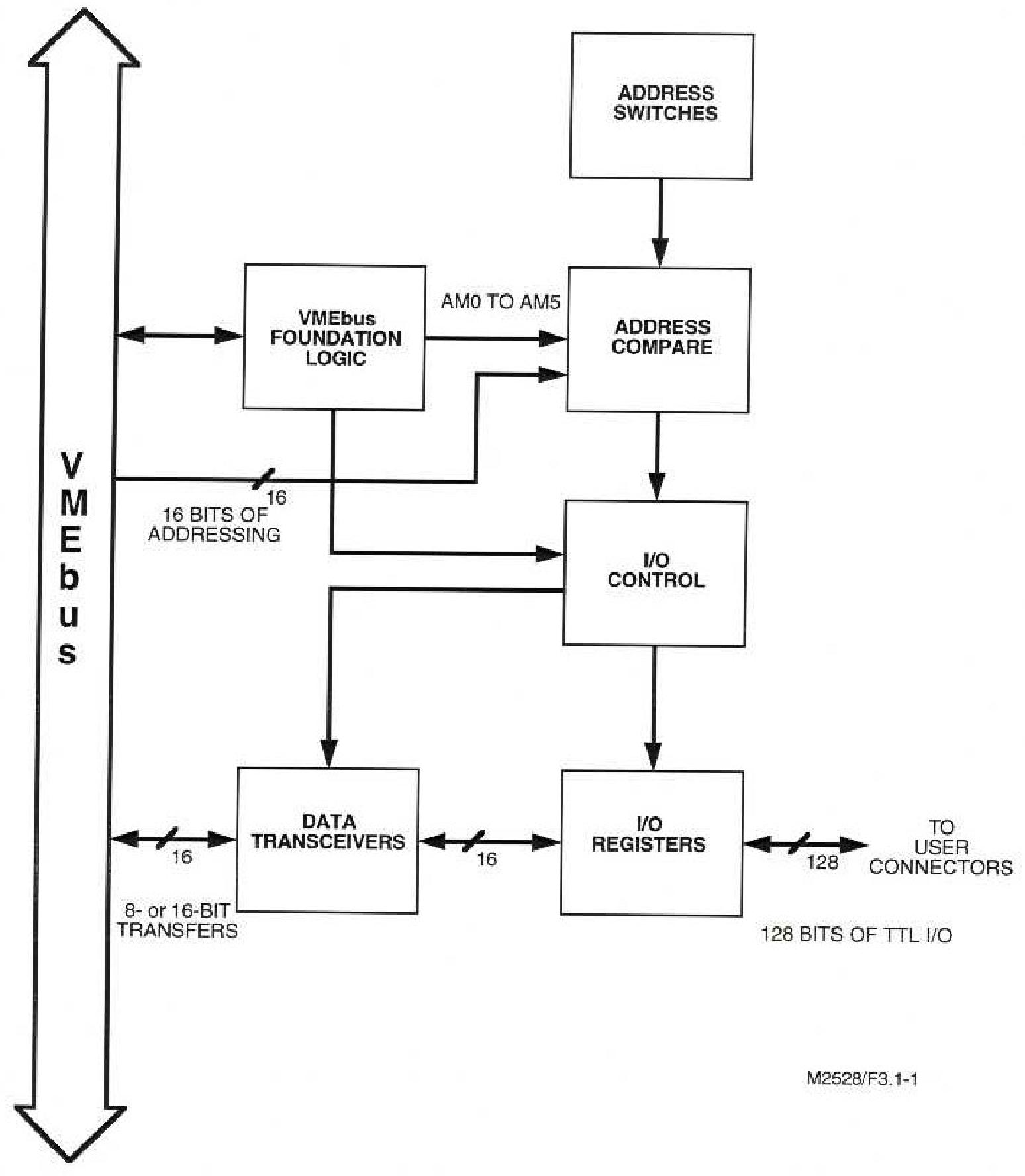
Block diagram: The functional block diagram is divided into six sub parts: VMEbus basic logic, data transceiver, address comparison logic, read/write register control logic, registers 0-3, and registers 4-7. There are also multiple subsystem block diagrams
Board addressing: supports data transmission of monitoring or non privileged short I/O memory space, selects I/O access type through jumper, factory configured to respond to short monitoring I/O access, and has two board selection DIP switches for setting the board's base address
VMEbus basic logic: including typical VMEbus drivers, receivers, and control logic
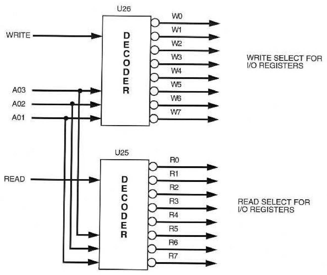
Register read/write control logic: Address bits A01, A02, A03 and read/write control lines are decoded into eight write control lines and eight read control lines, routed to the enable pins of each bidirectional latch, which can be selected for read or write operations through jumper wires
Data transmission description: The corresponding I/O data register is selected for data transmission through address bits A3, A2, and A1 combined with a data gating signal. The board selection signal generates an active signal for data transmission with DSO and DS1 logic gates. The board selection also activates a delay signal to generate a delayed version, which is used to provide setup time for the data transceiver during the write cycle before locking the data into the I/O register. The DTACK signal indicates that the data has been latched (write cycle) or is valid (read cycle)
I/O port enable description: The system reset signal (powered on or initiated by the VMEbus master device) disables all I/O ports/registers, and enables all I/O ports by writing to the I/O register R7L, regardless of whether they are configured as input or output ports
Programming
I/O register mapping: 12 bit addresses (A15 to A04) are used for board selection decoding, and the address switch is set to match these bits to generate data transfer board selection signals. The 128 bit I/O is divided into eight 16 bit registers for word transfer, and address bits A03, A02, and A01 are used to decode one of the eight registers, with a detailed I/O register mapping table
I/O port direction: Programming should be consistent with the I/O configuration selected by the jumper in the I/O port direction. The output port can only write data, and the input port can only read data. Please refer to Section 5 for jumper configuration details
Configuration and installation
Unpacking procedure: Product components may be sensitive to electrostatic discharge, unused boards should be stored in their original packaging, and it is recommended to use conductive materials when placing them. After receiving them, check for any transportation damage and handle them promptly
Physical installation: Power off installation or removal of the board, insert the board into the appropriate slot of the chassis, ensure correct alignment and orientation
Jumper and switch positions: Refer to Figure 5.3-1 for information on jumper and switch positions
I/O port direction jumper configuration: Table 5.4-1 specifies the use of jumpers J10 to J25, and installing jumpers will configure the corresponding ports as input ports
Address modifier: Factory configured to respond to short monitoring I/O access, installing jumper J9 can be changed to respond to short non privileged I/O access
Address selection switch: There are two address selection switches on the board, and Figure 5.6-1 shows their use in the addressing scheme
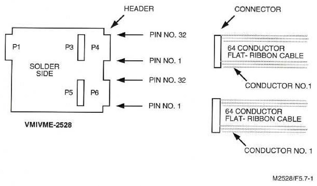
I/O cable and card edge connector configuration: The I/O connectors (P3 to P6) are 64 pin DIN standard, designed with high-quality ground planes connected to VMEbus ground and alternating I/O pins for connectors. They support connection to connectors P3, P4, P5, and P6 through four cables and have connector pin/channel allocation tables
Maintenance
Maintenance points: When the product malfunctions, it is necessary to check the software, system configuration, electrical connections, jumper or configuration options, whether the board is fully inserted, whether the connector pins are clean, whether adjacent board components are interfered with, cable and I/O connection quality, etc. If it needs to be returned for repair, it is necessary to contact VMIC to obtain a Return Merchandise Authorization (RMA) number
- OMRON
- ABB
- General Electric
- EMERSON
- Honeywell
- HIMA
- ALSTOM
- Rolls-Royce
- MOTOROLA
- Rockwell
- Siemens
- Woodward
- YOKOGAWA
- FOXBORO
- KOLLMORGEN
- MOOG
- KB
- YAMAHA
- BENDER
- TEKTRONIX
- Westinghouse
- AMAT
- AB
- XYCOM
- Yaskawa
- B&R
- Schneider
- KONGSBERG
- NI
- WATLOW
- ProSoft
- SEW
- ADVANCED
- Reliance
- TRICONEX
- METSO
- MAN
- Advantest
- STUDER
- DANAHER MOTION
- Bently
- Galil
- EATON
- MOLEX
- DEIF
- B&W
- ZYGO
- Aerotech
- DANFOSS
- Beijer
- Moxa
- Rexroth
- Johnson
- WAGO
- TOSHIBA
- BMCM
- SMC
- HITACHI
- HIRSCHMANN
- Application field
- XP POWER
- CTI
- TRICON
- STOBER
- Thinklogical
- Horner Automation
- Meggitt
- Fanuc
- Baldor
- SHINKAWA
- Other Brands
- UniOP
- KUKA
- Iba
- Beckhoff
- ADLINK
-
 Rolls Royce H1111.0204 Ship Main Controller
 -
 Basler Electric BE3-32-3AC Reverse Power Relay 9 1376 00 105
 -
 Basler Electric BE3-25-1A1N4 Synch Check Relay 9319100100
 -
 Basler Electric SR4A-2B15B3A Static Voltage Regulator
 -
 Basler Electric SR4A-2B15B3E Static Voltage Regulator
 -
 Basler Electric 9170818100 Solid State Protective Relay
 -
 Basler Electric AEC63-7 Analog Excitation Controller
 -
 Basler Electric 17483 Auxiliary Module
 -
 Basler Electric BE1-59 Over Voltage Relay
 -
 Basler Electric 21600-101 Control Module
 -
 Basler Electric KR2F Generator Voltage Regulator 9056600100
 -
 Basler BE1-CDS Current Differential System
 -
 Basler Electric CBS 212 Current Boost System 9 2650 00 100
 -
 Basler Electric IFM-150 Firing Circuit Chassis
 -
 Basler Electric BE1-60 Voltage Balance Relay C1F A1P D0C3F
 -
 Basler Electric BE1-32R Power Relay A2E D1R A0N0F
 -
Basler Electric BE1-32R Power Relay A2E D1R A0N0F
-
 Basler Electric 8650C80G01 Isolation Transducer PCB Board
 -
 ETEL EA-P2M-300-4/7.5A-0100-01 AccurET Modular 300 Servo Drive
 -
 Basler Electric 87T Transformer Differential Relay
 -
 Basler Electric BE-6868 Power Transformer 5950007559202
 -
 Basler Electric PRS250 Veri-Sync Relay 9088800102
 -
 Basler Electric SCP-250-G-60 VAR Power Factor Controller
 -
 Basler DECS-150 AVR 1NS2V1N1S Voltage Regulator
 -
 Basler UFOV 260A Under Frequency Overvoltage Module
 -
 Basler MOC2 199 Motor Operated Control – Overview and Setup
 -
 Basler BE3-49R-5K5A1 Temperature Relay – Complete Guide
 -
Basler BE 20035 001 Transformer – Technical Data and Installation
-
 Basler BE 02727 001 Transformer – Specifications and Usage
 -
 Basler BE127 Under Voltage Relay – Features and Application Guide
 -
Basler CBS377 Current Boost System – Complete Technical Guide
-
 Basler BE1-87G P/N 9170818100 Differential Relay – In-Depth Specs
 -
Basler BE1-87G Generator Differential Relay – Technical Overview
-
Basler Electric SR4A2B16 SVR Static Voltage Regulator – Complete Guide
-
 Basler Electric 9261500101 Power Supply Module
 -
 Basler Electric AEM-2020 Analog Expansion Module
 -
Basler Electric DGC-2020 Digital Genset Controller 51BRBNEAH001
-
Basler Electric BE1-59N Ground Fault Overvoltage Relay
-
 Basler Electric BE1-59N-A5E-E1L-N0S1F Neutral Overvoltage Relay
 -
Basler Electric MOC2499 Motor Operator Control Potentiometer 9072300430
-
 Basler Electric BE1-50/51M Overcurrent Relay
 -
 Basler Electric 9148100106 MOC3502 Solid State Relay 250VDC 0.25A
 -
 Basler Electric CBS 212 Current Boost System 9265000100
 -
 Basler Electric 10493002 Control Module
 -
Basler BE1-32R D3E E1R A0N1F Power Relay
-
 Basler SR8A2B15B3A Static Voltage Regulator
 -
 Basler IFM-105 Firing Circuit Chassis 9324100105
 -
Basler SR4A2B05B3A Static Voltage Regulator
-
 Basler BE151G1EB6PB0N0F Protective Relay
 -
Basler BE1-59 Electric Over Voltage Relay
-
 Basler 277 Static Programmable Powerline Carrier Channel
 -
 Basler BE1-32R D1E A1P A0N1F Power Relay
 -
Basler SR4A1B07B3A Static Voltage Regulator
-
 Basler Electric BE1-700 Digital Protective Relay
 -
Basler Electric SR8A-2B01B3A Static Voltage Regulator
-
 Basler Electric SR4A-2B01B3E Static Voltage Regulator
 -
 Basler Electric 9017709102 PC Board
 -
Basler Electric SR4A-2B01B3A Static Voltage Regulator
-
 Basler Electric PRS-250 Veri-Sync Relay
 -
 Basler Electric 9066800102 Excitation Support System
 -
Basler Electric BE1-87G Generator Differential Relay 9 1708 18 100
-
 Basler Electric 36T865-2 BE03752001 Power Supply
 -
 Basler Electric M-300 149D940G02 Power Supply
 -
 Basler Electric ACA2040-25GM 4Mp 25Fps Area Scan Camera
 -
 Basler BE1-87G-S1A-A1C-A0N0 Differential Relay
 -
Basler SR8A-2B06B3E Static Regulator SR8A2B06B3E
-
 Basler SCP-210 Frequency Controller 9095400100
 -
 Basler BE1-59-A3E-A1J-N1N3F Overvoltage Relay BE159A3EA1JN1N3F
 -
Basler 9 2011 11 100 Bracket Mounted Terminal Unit
-
Basler 9 1606 00 101 Voltage Regulator
-
 Basler CBS-377 Current Boost System 9109600102
 -
 Basler 8650C72 Exciter Control Module PCB Rev 5
 -
 Basler C2EE1PA0N1F BE1-32R Reverse Power Relay
 -
 ADLINK HPCI-14S12U - Industrial Control Backplane 12PCI Backplane PCI-14S Passive Backplane
 -
-0010.png) ADLINK PCIe-GIE74C - image acquisition card 4-CH GigE Vision PoE+ Frame Grabber
ADLINK PCIe-GIE74C - image acquisition card 4-CH GigE Vision PoE+ Frame Grabber -
-0010_1.png) ADLINK PCI-8164 - control card 4-Axis Advanced Motion Controller Board
ADLINK PCI-8164 - control card 4-Axis Advanced Motion Controller Board -
 ADLINK PCIe-U304 - 4 Port USB3 PCIe Frame Grabbers USB Screw Hole Card
 -
 ADLINK PCI-9112 - Multi-Function Data Acquisition Card DAQ Card
 -
 ADLINK PCI-7432 - 51-12013-0A50 4-CH Isolated Numérique I/O PCI Cartes Digital I/O Card
 -
 ADLINK PCA-6106P3-0C1 REV.C1 - backplane 6-Slot Passive Backplane Board
 -
 ADLINK PCI-7224 - 24-CH Opto-Isolated Digital I/O PCI Board
 -
 ADLINK CPCI-7433R(G) - Digital Input Board Rear I/O CompactPCI Card
 -
 ADLINK EBP-13E4 - 51-46703-0A30 Industrial PC Backplane Passive Backplane
 -
 ADLINK PCIE-HDV62 - Image acquisition card High Definition Video Frame Grabber
 -
 ADLINK EBP-13E4 - 51-46703-0A30 Industrial Backplane Board Passive Backplane
 -
 ADLINK 90111-B1 / CPCI-6770 - PCB CPU MODULE CompactPCI Single Board Computer
 -
 ADLINK PCI-7248 - DATA ACQUISITION PCI CARD 48-CH Parallel Digital I/O Board
 -
 ADLINK PCI-7230 - 51-12003-0a50 board PCI7230 32-CH Isolated Digital I/O Card
 -
 ADLINK PCI2A000CB - 51-20000-0B30 Multi-Function DAQ Card Baseboard
 -
 ADLINK PCI-8134-005 - 4-Axis Motion Controller Card
 -
 ADLINK PCI-7224 - 24-CH Opto-Isolated Digital I/O PCI Card
 -
 ADLINK PCI-7434 - 64-CH Isolated Digital Output Card
 -
 ADLINK PCI-8132 - motion control card 2-Axis Servo & Stepper Controller
 -
 ADLINK PCI-8134 - Motion Controller PCI Card 4-Axis Controller Board
 -
 ADLINK PCI-8164 - Motion Control Card 51-12406-0A40 4-Axis Controller
 -
 ADLINK 51-12001-0C20 - Circuit Board Data Acquisition Interface Module Hardware
 -
 ADLINK NuPR0-840 - industrial control motherboard Full-Size PICMG CPU Board
 -
 ADLINK PCI-7444 - 51-12023-0A10 card 128-CH Isolated Digital Output Board
 -
 ADLINK PCI-1612B - data acquisition card 4-Port RS-232/422/485 Serial Communication Card
 -
 ADLINK PCI-6208V 009 - 8/16-CH 16-Bit Analog Output Cards PCB-I-E-482=6BX3
 -
 ADLINK NUPRO-935A/LV - industrial control motherboard Full-Size PICMG SBC Board
 -
 ADLINK PCI-9114DG - Multi-Function DAQ Card Data Acquisition PCI Card
 -
 ADLINK ACL-7130 - Data acquisition card Isolated Digital I/O Board
 -
 ADLINK ABX-6300D-4E1-BP - board ABX6300D4E1BP Video Interface Expansion Card
 -
 ADLINK CPCI-6940 - CPCI-6940/D1539/M16-0(EA)-000E 6U CompactPCI Processor Board
 -
 ADLINK NuPRO-760 - industrial control motherboard Half-Size PICMG SBC CPU Board
 -
 ADLINK IMB-M42H (G)-0020 - industrial control motherboard LGA1155 Micro-ATX Mainboard
 -
 ADLINK RTV-24 / PCI-MP4S - 51-12519-1C30 4-Channel Real Time Video Capture Board
 -
 ADLINK PCI-8134 - 4-Axis Servo & Stepper Motion Controller Card
 -
 ADLINK MXC-6101D - V.PC000.002.ST.00 Box PC Configurable Embedded Computer
 -
.png) ADLINK PCI-8134A - 51-12421-0A10 Motion Control Card 4-Axis Controller Card
ADLINK PCI-8134A - 51-12421-0A10 Motion Control Card 4-Axis Controller Card -
 ADLINK DIN-100S / DIN-100SA1 - Technology SCSI-II TB 100-PIN Terminal Block Board
 -
.png) ADLINK DIN-812M001 / DIN812M001 - 51-14034-0A1 51140340A1 Terminal Module Breakout Interface
ADLINK DIN-812M001 / DIN812M001 - 51-14034-0A1 51140340A1 Terminal Module Breakout Interface -
_1.png) ADLINK PCI-8164 - Servo motion control 4-Axis Advanced Controller Card
ADLINK PCI-8164 - Servo motion control 4-Axis Advanced Controller Card -
 ADLINK PCIe-GIE64 - Acquisition card GigE Vision PoE+ Frame Grabber
 -
 ADLINK M-302 - Industrial control motherboard ATX PC Board Mainboard
 -
 ADLINK PCI-8134 - Motion Controller PCI Card 4-Axis Controller Board
 -
 ADLINK PCI-RTV24 - Image capture card Analog Video Frame Grabber
 -
 ADLINK PCI-8102 - Motion control card 2-Axis Servo & Stepper Controller Board
 -
 ADLINK PCI-9112 REV.B1 - Card Multi-Function Data Acquisition Card
 -
 ADLINK HSI-DI32-M-N / HSL-TB32-M-DIN - Discrete I/O MODULE Distributed Automation Module System
 -
 ADLINK PCI-7296 - IO card REV.A3 96-CH Parallel Digital I/O Card
 -
-0020.png) ADLINK DIN-814P-A4 / 814Y - terminal board Motion Control Interface Block
ADLINK DIN-814P-A4 / 814Y - terminal board Motion Control Interface Block -
 ADLINK DIN-814P-A4 - 51-14056-0A10 PCB-I-E-2736=ZA01 Screw Terminal Board Breakout
 -
 ADLINK M-322 - motherboard Industrial Control Computer Mainboard
 -
 ADLINK NUPRO-406 REV:B1 - industrial control motherboard Full-Size PICMG CPU Board
 -
 ADLINK AMP-204C - card DSP-Based 4-Axis Advanced Pulse-Train Controller
 -
 ADLINK HPCI14S REV.B1 - industrial computer baseboard 14-Slot Passive Backplane


