
TOSHIBA VF-AS3 inverter RS485 communication function
Core purpose: To achieve three major functions through RS485 bus - remote control (run/stop, frequency setting, torque adjustment), parameter reading and writing (internal parameter configuration of frequency converter), and status monitoring (output frequency/current/voltage, fault code, terminal status), supporting master-slave synchronous control between frequency converters without relying on PLC or upper computer.
TOSHIBA VF-AS3 inverter RS485 communication function
Basic Information and Security Standards for Documents
1. Scope of application and core purpose
Applicable equipment: Toshiba VF-AS3 series full specification frequency converter, covering 200V level (0.4-55kW) and 400V level (0.4-280kW, including IP55 protection type), supporting 2 independent RS485 communication interfaces (Connector1/Connector2).
Core purpose: To achieve three major functions through RS485 bus - remote control (run/stop, frequency setting, torque adjustment), parameter reading and writing (internal parameter configuration of frequency converter), and status monitoring (output frequency/current/voltage, fault code, terminal status), supporting master-slave synchronous control between frequency converters without relying on PLC or upper computer.
2. Safety and usage restrictions
Mandatory safety requirements:
It is prohibited to plug and unplug RS485 communication cables with power on, and it is forbidden to connect Ethernet signals to the RS485 interface, otherwise it may cause the communication module to burn out or the frequency converter to malfunction.
Communication timeout parameters (F803/F823) must be set to avoid device loss of control during communication interruption. After timeout, "continue operation", "trip immediately", or "trip after deceleration" can be set (default to continue operation).
The limit for writing EEPROM is 100000 times (for parameter storage media), and there is no limit for writing RAM. It is recommended to use the P command to write frequently modified parameters (such as frequency commands) to RAM, and avoid writing frequently to EEPROM for parameters that do not need to be stored.
Usage restrictions:
The length of communication cables should match the baud rate (recommended ≤ 100m at 19200bps and ≤ 50m at 38400bps), and repeaters should be added for long distances.
The same RS485 bus can connect up to 32 devices, and the frequency converter number (F802) must be unique (0-247) and must not be duplicated.
Hardware wiring and transmission specifications
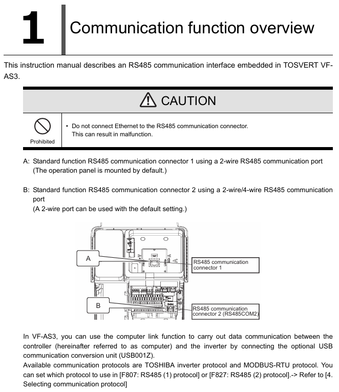
1. Definition of communication interface pins
VF-AS3 is equipped with two RS485 interfaces (Connector1/Connector2), both of which are RJ45 interfaces. The pin functions are as follows (key pins are bolded):
(1) Connector1 (default 2-wire system, non switchable)
Pin number, signal name, function description, wiring requirements
1/2/6- Reserved pins must not be connected to any cables, otherwise communication signals may be short circuited
4 RXA+/TXA+non-polar transmission and reception data positive terminal is connected to bus A line (usually red), and all devices are interconnected through this pin
5 RXB -/TXB - Non polarized transmission and reception data negative terminal connected to bus B line (usually blue), this pin is interconnected for all devices
7 Power pins are prohibited from connection to avoid power conflicts and burning interfaces
All devices with SG signal ground are interconnected with SG pins, and ultimately grounded at a single point (ground resistance ≤ 4 Ω)
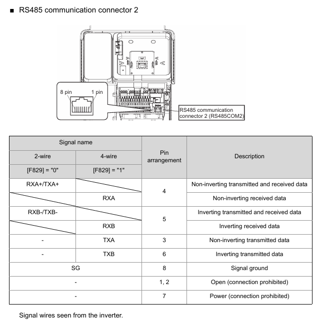
(2) Connector2 (supports 2-wire/4-wire system, [F829] parameter switching)
Pin number 2-wire system function ([F829]=0) 4-wire system function ([F829]=1) wiring requirements
1/2- Reserved pins suspended, wiring prohibited
3- TXA+(transmitting data positive end) is only used by the 4-wire master station and connected to the RXA slave station+
RXA+/TXA+(transmit/receive positive terminal) RXA+(receive data positive terminal) 2-wire system is the same as Connector1; 4-wire system connected to the main station TXA+
5 RXB -/TXB - (transmit/receive negative terminal) RXB - (receive data negative terminal) 2-wire system is the same as Connector1; 4-wire system connected to the main station TXB-
6-TXB - (transmitting data negative terminal) is only used by the 4-wire master station and connected to the RXB slave station-
7 Power pins are prohibited from connection
8 SG signal ground interconnected with all equipment SG, single point grounding
2. Wiring specifications and hardware configuration
(1) Cable requirements
Shielded twisted pair cables must be used, with a conductor cross-sectional area of ≥ 0.22mm ² (AWG24) and a characteristic impedance of 100-120 Ω (matching RS485 bus impedance). The shielding layer needs to be grounded at both ends (if cross device grounding is required, equipotential bonding wires should be used to avoid ground current).
The distance between communication cables and the main circuit cables of the frequency converter (3-phase power supply and motor wires) should be ≥ 20cm. Parallel wiring or sharing of the same cable tray is prohibited to reduce electromagnetic interference (EMI).
(2) Required resistor configuration (cannot be omitted)
The stable operation of RS485 bus requires two types of resistors, and all nodes must be configured with:
Terminal resistance: 120 Ω/1/2W, only connected between the A+/B - pins of devices at both ends of the bus (such as the leftmost and rightmost frequency converters), to suppress signal reflection and avoid data transmission distortion.
Up and down resistors: 510 Ω/1/2W, each device's A+pin is connected to a 510 Ω resistor to+5V (or the positive terminal of the power supply), and the B - pin is connected to a 510 Ω resistor to GND. The purpose is to enhance the bus driving capability and avoid communication packet loss when weak signals occur.
(3) 2-wire and 4-wire wiring examples
2-wire system (default, recommended): A+(4-pin) interconnection, B - (5-pin) interconnection, SG (8-pin) interconnection for all devices, with 120 Ω terminal resistors connected at both ends of the bus and pull-down resistors connected at each node.
4-wire system (requires [F829]=1): The TXA+(3-pin)/TXB - (6-pin) of the master station is connected to the RXA+(4-pin)/RXB - (5-pin) of all slave stations, and the slave stations have no transmit pin (no response). The rest is the same as the 2-wire system, suitable for master-slave unidirectional communication and high reliability scenarios.
3. Transmission specification parameters
Transmission parameter support options default values note
Half duplex transmission method - can only receive or send data at the same time to avoid conflicts
Synchronization mode start and end synchronization - identify the beginning and end of frames by "3.5 byte blank time" (9600bps ≈ 4ms, 19200bps ≈ 2ms, 38400bps ≈ 1ms)
The baud rate is 9600bps/19200bps/38400bps. After modifying 19200bps, it needs to be powered off and reset to take effect. All bus devices must be consistent
No parity check/even parity check/odd parity check. After modifying the parity check, it needs to be powered off and reset to take effect. It is recommended to use even parity check (with strong anti-interference ability)
8-bit data bit (ASCII: JIS X0201; Binary/MODBUS: fixed 8-bit) - no options, non modifiable
Stop bit reception: 1 bit; Sending: 2 bits - compatible with upper computer 1/1.5/2 bit stop bit settings, no adaptation required
Error detection Toshiba protocol: checksum (optional); MODBUS-RTU: CRC16 (required) - When verifying an error, the frequency converter does not respond, and the upper computer needs to resend it
Detailed explanation of communication protocol (dual protocol support)
VF-AS3 supports two communication protocols, which can be switched through parameters [F807] (Connector1)/[F827] (Connector2). The default is the "Toshiba Inverter Protocol", and two protocols (different interfaces) can be enabled simultaneously.
1. Toshiba inverter protocol (native protocol, with the most comprehensive functions)
Supports ASCII, Binary, and block communication modes, accessing inverter parameters through a "communication number" (4-digit hexadecimal). The command set covers read, write, and inter inverter communication, making it suitable for Toshiba device networking.
(1) ASCII mode (suitable for PC/PLC, with strong readability)
Frame format (computer → frequency converter): (INV-NO CMD communication number DATA&SUM) CR
Initial code: "(" (28H), final code: ")" (29H)+CR (0DH), cannot be omitted.
INV-NO: Inverter number (2-digit ASCII, 00-99, "* *" represents broadcast).
CMD: Command code (R=Read, W=Write RAM+EEPROM, P=Write RAM, G=Read (2-wire system specific)).
Communication number: 4-digit hexadecimal (e.g. FD00=output frequency, FA01=frequency command).
SUM: checksum (2-digit ASCII, optional), calculated as "the last two digits of the sum of all ASCII codes between the header and&".
Example: Set the frequency to 60Hz (communication number FA01, 60Hz=1770H)
Command: (00PFA011770) CR (00=inverter number, P=write to RAM, 1770=hexadecimal corresponding to 60Hz).
Response: (00PFA011770) CR (The frequency converter returns the same command, confirming successful writing).
(2) Binary mode (suitable for microcontrollers/embedded systems, high transmission efficiency)
Frame format (computer → frequency converter):/INV-NO CMD communication number DATA SUM
Header code: "/" (2FH), no tail code, SUM (1 byte) is required.
INV-NO: Inverter number (1-byte hexadecimal, 00H-3FH, FFH=broadcast).
CMD: Command code (52H=R, 57H=W, 50H=P, 53H=S (between frequency converters)).
Communication number: 2-byte hexadecimal (high-order, such as FD00=output frequency).
SUM: checksum (1 byte), calculated as the last 8 bits of the sum of all bytes from the header to DATA.
Example: Read output frequency (communication number FD00)
Command: 2F 52 FD 00 82 (2F=/, 52=R, FD00=communication number, 82=SUM).
Response: 2F 52 FD 00 17 70 05 (1770H=6000 → 60.00Hz, 05=response SUM).
(3) Block communication mode (efficient batch read/write)
Core advantage: A single communication can simultaneously write 2 parameters and read 5 parameters, reducing the number of communication times and suitable for batch configuration or centralized monitoring scenarios.
Parameter preset: You need to first set the "block write parameters" (such as FA00=run command, FA01=frequency command) through [F870]/[F871], and set the "block read parameters" (such as FD00=output frequency, FD03=output current) through [F875] - [F879].
Frame format: Computer sends X command (58H), frequency converter sends Y command (59H), example:
Computer command: 2F 58 02 05 C4 00 17 70 D9 (02=write 2 parameters, 05=read 5 parameters, C400=forward command, 1770=60Hz).
Inverter response: 2F 59 05 00 64 00 17 70 1A 8A 24 FD 00 3D (returns 5 read parameter results, 64=100 → 60Hz, 1A8A=6794 → 67.94% current, etc.).
(4) Broadcast communication
Only supports write commands (W/P), does not support read commands, suitable for batch configuration of all devices.
ASCII mode: INV-NO is set to "* *" (such as (* * PFA011770) CR), only the device numbered 00 responds, and other devices do not respond when executing commands.
Binary mode: INV-NO is set to FFH, and only the device numbered 00 responds to avoid bus conflicts.
2. MODBUS-RTU protocol (compatible with third-party devices)
Only supports MODBUS-RTU subset (binary transmission), does not support ASCII mode, suitable for networking with third-party PLCs, touch screens, and other devices. The core instructions are as follows:
Instruction code (Hex) function description applicable scene frame format (computer → frequency converter)
03H Read Keep Register reads one or more parameters (indirect read ≤ 5, direct read ≤ 8) inverter number+03H+communication number (high-order)+read word count (high-order)+CRC16
Write a single hold register in 06H and write one parameter (such as frequency instruction, run command): frequency converter number+06H+communication number (high-order first)+write data (high-order first)+CRC16
10H write multiple hold registers, write 2 or more parameters (such as block write preset parameters), inverter number+10H+communication number (high-order)+write word count (high-order)+data byte count+write data+CRC16
Write and read multiple registers in 17H, simultaneously write parameters+read parameters (such as write frequency+read output current), inverter number+17H+read communication number+read word count+write communication number+write word count+data byte count+write data+CRC16
2BH reads model information, manufacturer, model, and version (such as "TOSHIBA" and "VFAS3-2037P"), inverter number+2BH+MEI type (0EH)+equipment code+object code+CRC16
(1) CRC16 Calculation Rule (Required)
The CRC16 of MODBUS-RTU is a 16 bit checksum, and the calculation steps are as follows:
Initialize the CRC register to FFFFH;
XOR the data byte by byte with the CRC register;
Shift each byte by 1 bit to the left. If the lowest bit is 1, XOR the CRC register with polynomial A001H;
Repeat step 3 8 times to process all bytes;
The final CRC value is stored at the end of the frame with "low bits first, high bits second".
Example: The CRC16 of the command "01 03 FD 00 00 01" is B5A6H, and the complete command is "01 03 FD 00 01 B5 A6".
(2) Example: Read output frequency (communication number FD00)
Inverter parameters: Number 1 (01H), baud rate 19200bps, even parity.
Computer command: 01 03 FD 00 00 01 B5 A6 (01=number, 03=read, FD00=communication number, 0001=read 1 parameter).
Inverter response: 01 03 02 17 70 B6 50 (02=number of data bytes, 1770H=6000 → 60.00Hz, B650=CRC16).
Core function: master-slave communication between frequency converters
Without the need for an upper computer, synchronous control of one master and multiple slaves can be achieved through the RS485 bus, which only supports Toshiba inverter protocol. The main station sends S command (53H), and the slave station does not respond when receiving commands, avoiding bus conflicts.
1. Master slave parameter configuration (key parameters)
Example Setting of Character Core Parameter Configuration Options (45Hz Output from the Station)
Master station [F806]/[F826] (master-slave mode) 3=frequency command, 4=output frequency, 5=torque command, 6=output torque [F826]=3 (frequency command)
Main station [F805]/[F825] (transmission waiting time) 0.00-2.00s (default 0.00s) 0.01s (to avoid the main station sending too fast)
Slave station [F806]/[F826] (master-slave mode) 0=0Hz in case of fault, 1=continue operation in case of fault, 2=emergency stop in case of fault [F826]=0 (fail safe)
From station [F823] (communication timeout) 0.1-100.0s (default 0.0s disabled) 1.0s (tripped when cable disconnected)
Slave [FMOd] (frequency command source) 21=Connector1, 22=Connector2 22 (same interface as the master station)
Slave [FH] (maximum frequency) 0.0-400.0Hz 90.0Hz (target maximum frequency)
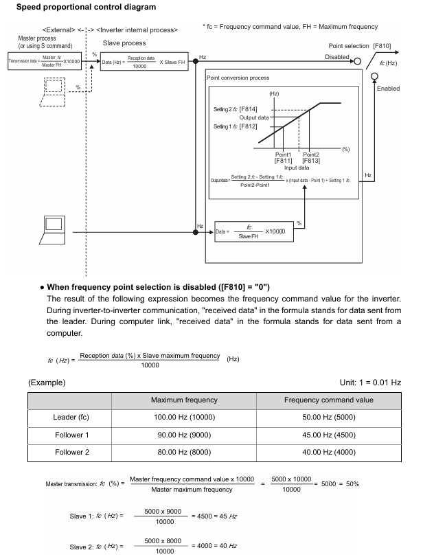
2. Speed proportional control logic
The frequency of the slave station is calculated according to the proportion of the master station's instructions, and supports two modes: "no correction" and "two-point correction":
(1) No calibration mode (F810=0)
Calculation formula: Slave frequency (Hz)=(Master command value (%) x Slave maximum frequency (Hz))/10000
Main station command value: 1%=100 (e.g. 50%=5000), main station frequency command=(actual frequency of main station x 10000)/maximum frequency of main station.
Example: The maximum frequency of the main station is 60Hz, and the actual output is 30Hz → Main station command=(30 × 10000)/60=5000 (50%); The maximum frequency of the slave station is 90Hz → the slave station frequency=(5000 × 90)/10000=45Hz.
(2) Two point correction mode ([F810]=1, non-linear ratio)
Preset two parameters: [F811]=Point 1 command value (%), [F812]=Point 1 frequency (Hz); [F813]=Point 2 command value (%), [F814]=Point 2 frequency (Hz).
Calculation formula: Slave frequency=Point 1 frequency+(Main station instruction - Point 1 instruction) × (Point 2 frequency - Point 1 frequency)/(Point 2 instruction - Point 1 instruction)
Example: Point 1 (0% → 10Hz), point 2 (100% → 80Hz), master station instruction 50% → slave station frequency=10+(50-0) × (80-10)/(100-0)=45Hz.
3. Fault handling
Main station tripping: The main station sends the command s (73H), and the slave station sets the action according to [F806]/[F826] (0=0Hz, 1=continue operation, 2=emergency stop).
Communication interruption: The communication timeout (Err5) is triggered by the slave station, and the action (such as tripping) is set according to [F824]. The master station is not affected (the status needs to be fed back through the FL fault terminal of the slave station).
Detailed explanation of communication related parameters
The communication function of the frequency converter requires the configuration of a "communication parameter group" (F8xx series), and some parameters need to be reset after power failure to take effect. The key parameters are as follows:
Parameter number, parameter name, function description, adjustment range, default value, effective method
F800/F820 RS485 baud rate setting communication rate 0=9600bps, 1=19200bps, 2=38400bps 1 (19200bps) power off reset
F801/F821 RS485 checksum setting verification method 0=no verification, 1=even verification, 2=odd verification 1 (even verification) power off reset
F802 frequency converter number setting bus address 0-247 0 immediately
F803/F823 communication timeout setting timeout detection duration 0.0 (disabled), 0.1-100.0s 0.0s immediately
F804/F824 timeout operation timeout device action 1=continue running, 4=trip immediately, 6=trip immediately after deceleration, 1=trip immediately
F806/F826 master-slave communication mode setting master-slave role master station: 3-6; Slave: 0-20 (Slave) Power off reset
F807/F827 communication protocol selection Toshiba/MODBUS 0=Toshiba protocol, 1=MODBUS-RTU 0 power-off reset
F829 RS485 (2) wiring type 2-wire/4-wire switching 0=2-wire system, 1=4-wire system 0 immediately
F830 MODBUS continuous address direct read whether to skip empty parameter 0=skip, 1=do not skip 0 immediately
F870/F871 block write parameter 1/2 setting block communication write parameter 0=disabled, 1=FA00 (run command), etc. 0 power off reset
F875-F879 block read parameters 1-5 set block communication read parameters 0=disabled, 1=FD01 (status), etc. 0 power off reset
Troubleshooting and Appendix
1. Common faults and solutions
Troubleshooting steps for possible causes of fault phenomena
Communication unresponsive 1. Baud rate/checksum/protocol mismatch; 2. Wiring error (A+/B - reversed connection, SG not connected); 3. The frequency converter number does not match; 4. Uninnected terminal/pull-up/pull-down resistor 1. Unify all device parameters (such as 19200bps+even parity+Toshiba protocol); 2. Check the A+/B - wiring to ensure SG interconnection; 3. Confirm that INV-NO is consistent with [F802]; 4. Install 120 Ω terminal resistors (at both ends) and 510 Ω pull-up and pull-down resistors (at all nodes)
Err5 tripped (communication timeout) 1. Communication cable disconnected; 2. The main station did not send data; 3. The timeout period is too short; 4. The slave station did not receive the command from the master station. 1. Check the continuity of the cable; 2. Confirm that the main station sends commands normally (such as once per second); 3. Increase [F823] (e.g. set to 1.0s); 4. Verify the master and slave station interfaces (if both are using Connector2)
Write parameter error (N0000): 1. During operation, write prohibited parameters (such as maximum frequency [FH]); 2. Parameter locking ([F700]=2/4); 3. Password setting ([F738]) 1. Write prohibition parameter after shutdown; 2. Set [F700]=0 (unlock); 3. Clear the [F738] password
Data transmission error (garbled code) 1. Electromagnetic interference (parallel wiring with the main circuit); 2. Cable over distance; 3. The terminal resistor is not connected. 1. Adjust the cable routing and keep it away from the main circuit; 2. Shorten cables or add repeaters; 3. Connect a 120 Ω terminal resistor
2. Appendix Key Information
(1) Response time calculation
Total response time=data communication time+frequency converter processing time (maximum 10ms).
Data communication time=(bytes x bits)/baud rate, bits=1 (start bit)+8 (data bit)+1 (check bit)+2 (stop bit)=12 bits (default).
Example: 19200bps, 8-byte command → communication time=(8 × 12)/19200=5ms, total response time ≈ 15ms.
(2) Corresponding Table of Inverter Models and FB05 Parameters
[FB05] The parameter is used to identify the frequency converter model, and some common models correspond to the following relationships:
Inverter model, voltage level, power FB05 (decimal), FB05 (hexadecimal)
VFAS3-2037P 200V 3.7kW 9 9
VFAS3-4055PC 400V 5.5kW 42 2A
VFAS3-4220PCE 400V(IP55) 22kW 147 93
(3) ASCII code table
Provide JIS X0201 ASCII code mapping, such as "0"=30H, "A"=41H, "d"=64H, for ASCII mode command writing and data parsing.
- OMRON
- ABB
- General Electric
- EMERSON
- Honeywell
- HIMA
- ALSTOM
- Rolls-Royce
- MOTOROLA
- Rockwell
- Siemens
- Woodward
- YOKOGAWA
- FOXBORO
- KOLLMORGEN
- MOOG
- KB
- YAMAHA
- BENDER
- TEKTRONIX
- Westinghouse
- AMAT
- AB
- XYCOM
- Yaskawa
- B&R
- Schneider
- KONGSBERG
- NI
- WATLOW
- ProSoft
- SEW
- ADVANCED
- Reliance
- TRICONEX
- METSO
- MAN
- Advantest
- STUDER
- DANAHER MOTION
- Bently
- Galil
- EATON
- MOLEX
- DEIF
- B&W
- ZYGO
- Aerotech
- DANFOSS
- Beijer
- Moxa
- Rexroth
- Johnson
- WAGO
- TOSHIBA
- BMCM
- SMC
- HITACHI
- HIRSCHMANN
- Application field
- XP POWER
- CTI
- TRICON
- STOBER
- Thinklogical
- Horner Automation
- Meggitt
- Fanuc
- Baldor
- SHINKAWA
- Other Brands
- UniOP
- KUKA
- Iba
- Beckhoff
-
 Basler BE1-25 Time Overcurrent Relay M1FA6PA4S0F
 -
 Basler SR4A2B05B3E Static Voltage Regulator
 -
 Basler DECS-200-2L Digital Excitation Control
 -
 Basler BE303280001 Control Transformer
 -
 Basler 9262103004 Voltage Regulator Board For Basler DECS-400
 -
 Basler ICRM-7 Inrush Current Reduction Module
 -
 Basler BE1-32R Power Relay
 -
 BASLER ELECTRIC KR4F VOLTAGE REGULATOR 9042600100 600V 50/60Hz
 -
 Basler 9222600101 Power Module
 -
 Basler SR8A-2B15B3A Static Voltage Regulator
 -
 BASLER BE1-87G G1E A1L A0N1P Generator Differential Relay w/ Reactor 9170818100
 -
Basler 9284900101 DECS Power Module
-
 Basler PRS250 Veri-Sync Relay
 -
 Basler BE 12296 001 Transformer
 -
 Basler 905970-104 Rev.M Voltage Regulator
 -
Basler BE1-87T Transformer Differential Relay
-
 Basler SR8A-2B15B3A Static Voltage Regulator
 -
 Basler SR32A2B05B3E Static Voltage Regulator
 -
 Basler SR4A-2B16B3A Static Voltage Regulator
 -
 Basler SR32A-2B13B3E Static Voltage Regulator
 -
 Basler KR4F Voltage Regulator 9042600100
 -
 Basler SSR 32-12 Static Voltage Regulator 400Hz
 -
 Basler CBS 212A Current Boost System
 -
 Basler MVC236 Manual Control Module
 -
Basler UFOV Protective Module 9040000100
-
 Basler SSR 125-12 Static Voltage Regulator
 -
 Basler SR4A2B10A3E Static Voltage Regulator
 -
 Basler BE1-25 Solid State Time Overcurrent Relay
 -
 Basler MVC 232 Manual Voltage Control Module
 -
Basler PRS 250 Veri-Sync Relay
-
 Basler UFOV 260A Under Frequency Over Voltage Relay
 -
 Basler RUL2098-10GC Load Relay
 -
 Basler 9 1049 04 100 PC Board
 -
Basler 125-12 Static Voltage Regulator
-
Basler PRS 250 Veri-Sync Relay
-
Basler 9185900102 SSR 125-12 Regulator
-
Basler BE12819001 Reactor
-
 Teradyne 535-100-00 Power Supply
 -
 Basler BE1-67 Directional OC Relay
 -
 Basler PRP110 Reverse Power Relay
 -
 Basler BE30631001 Isolation Transformer
 -
 Basler DECS-200-2L Digital Excitation Control
 -
 Basler BE1-47N Voltage Phase Sequence Relay
 -
 Basler AEC63-7 Analog Excitation Controller 220-277V
 -
Basler BE1-50/51B-107 Overcurrent Relay
-
 Basler Electric BE1‑32R BE1‑E1P‑BON0F Protective Relay
 -
Basler BE1-25 Solid State Time Overcurrent Relay M1EA6PA5S1F
-
 Basler MVC 232 Manual Voltage Control Module 90 37000 103 60VAC 55VDC
 -
Basler RAL6144-16GM Racer GigE Line Scan Camera
-
Basler SSR 63-12 Static Voltage Regulator
-
 Basler BE1-51A Overcurrent Relay
 -
Basler BE1-87T Solid State Protective Relay
-
Basler SR4A2B01B3A Static Voltage Regulator
-
 Basler SSR 32-12 Static Voltage Regulator
 -
 Basler TRR00696 Transformer 1KVA 115V
 -
 Basler DECS-100-B15 AVR Replacement
 -
Basler BE1-27 Under-Voltage Relay
-
 Basler ACA2000-50GM Interface Module
 -
 Basler AEC63-7 Analog Excitation Controller
 -
Basler PRS 250 Veri-Sync Relay
-
 Basler SR4A-2B15B3A Static Voltage Regulator
 -
Basler BE1-32R Power Relay
-
Basler SR8A-2B06B3E Static Voltage Regulator
-
Basler BE1-81 O/U Frequency Relay
-
 Basler BE1-51A-K2E-W6M-B1N0F Overcurrent Relay
 -
Basler BE1-851 Overcurrent Relay G3A1S1 – 48-125V AC/DC
-
 Basler BEI-51 Overcurrent Relay – NSN 5945-01-293-2363
 -
Basler Electric L301KC Protective Relay – L301KC
-
 Basler DECS-100-B15 Automatic Voltage Regulator – Generator AVR
 -
Basler SR4A-2B15B3A Static Voltage Regulator – SR4A2B15B3A
-
Basler UF 312 Under Frequency Protective Module – 9094700100
-
Basler Electric MVC 232 Manual Control Module – 60VAC 55VDC 20A
-
Basler PRS 250 Veri-Sync Relay – Generator Synchronizing Relay
-
 Basler DECS-100-A05 Digital Regulator Review
 -
 Basler AEM-2020 Analog Expansion Module Specs
 -
 Basler DECS-100-B15 Digital Excitation Specs
 -
Basler Electric 9125600106 Regulator Component
-
Basler BE1-51A-K1E-W6M-B1N0F Overcurrent Relay
-
 Basler MVC-301 MVC 300 Excitation Controller
 -
Basler SSR 32-12 Static Voltage Regulator
-
Basler 9-2849-00-101 Control Module
-
Basler BE1-51A Overcurrent Relay
-
 Basler BE1-51/27R Overcurrent Relay
 -
 Basler BE1-51 Overcurrent Relay
 -
 Basler SR8A-2B15B3A Static Voltage Regulator
 -
 Basler BE32965001 Transformer and Timer Board
 -
 Basler 9174700100 EL200-7 Excitation Limiter
 -
 Basler BE2000E AVR Voltage Regulator
 -
Basler BE1-87G Differential Relay
-
 Basler BE21834001 Generator Control Module
 -
Basler DECS-100-B15 AVR
-
 Basler D90 96801 100 PCB Card
 -
 Basler XR2002F Voltage Regulator (110 VAC, 48-480 Hz)
 -
 Basler SR8A-2B14B3A Regulator
 -
 Basler 9561500100 Module
 -
 Basler DECS-400 BE1-11 System
 -
 Basler DECS-100-B15 Excitation Control
 -
Basler SCP 210 Frequency Controller
-
Basler SR4A-2B15B3A Static Voltage Regulator
-
Basler BE1-32R Power Relay
-
 Basler PIA2400-17GM Power Interface Adapter
 -
 Basler MVC 232 Manual Voltage Control Module
 -
Basler SSR 32-12 Static Voltage Regulator
-
Basler 5MW AVR Generator Voltage Regulator
-
 Basler VR63-4B Voltage Regulator
 -
Basler DECS-100-A05 AVR for Engine Generator
-
Basler DECS-100-B15 Automatic Voltage Regulator
-
Basler BE1-32R Directional Power Relay
-
Basler BE1-87B Differential Relay
-
 Basler UFOV 260A Protective Module
 -
 Basler 9-2614-02-100 PCB Rev M
 -
Basler DECS-100-B15 Digital AVR
-
 Basler 9284900103 PS DECS-400N
 -
 Basler D4N3H1U Intertie Protection
 -
 Basler DECS-100-B15 A15 AVR
 -
 Basler KR4F Voltage Regulator
 -
 Basler BE26434 T14 Transformer
 -
 Basler SR8A-2B15B3A Regulator
 -
 Westinghouse 774B472A12 AR Relay
 -
Basler DECS-100-B15 AVR
-
Basler XR2002F Regulator 110V
-
Basler SR125-E Static Regulator
-
Basler SSR 125-12 Regulator
-
Basler MOC2599 Motor Pot
-
 Basler BE1-DFPR Feeder Relay
 -
 Basler CBS 305 Current Boost
 -
Basler BE1-25 AutoSync
-
Basler MVC 300 Voltage Control


