Motorola MVME6100: High-Performance VME64 Computing
Next-Generation PowerPC Architecture for VMEbus
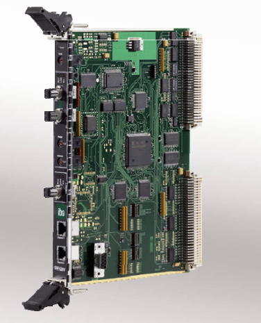
The Motorola MVME6100 represents the pinnacle of PowerPC-based VMEbus computing. Built to satisfy the demanding requirements of high-end embedded applications, it utilizes the Motorola MPC7457 processor. This processor is equipped with the AltiVec vector processing unit, which allows for highly parallelized math operations, making the MVME6100 an ideal platform for digital signal processing (DSP), image recognition, and complex simulation tasks. In an era where data throughput is as critical as raw processing speed, the MVME6100 introduces the 2eSST protocol, revolutionizing how data is moved across the VME backplane.
By integrating the Marvell Discovery III system controller, the MVME6100 optimizes the communication between the CPU, memory, and I/O subsystems. This high level of integration ensures that the processor is never "starved" for data, even when handling multiple high-speed Gigabit Ethernet streams and intensive PCI-X bus activity. The board is designed for a long lifecycle, providing a robust solution for industries such as defense, aerospace, and semiconductor manufacturing.
Technical Specification Overview
| Feature | Technical Detail |
|---|---|
| Microprocessor | MPC7457 PowerPC with AltiVec (1.25 GHz or higher) |
| Memory | Up to 2GB DDR ECC SDRAM |
| VME Interface | Tundra Tsi148 (Supports 2eSST at 320 MB/s) |
| PCI Expansion | Dual independent PCI-X buses (64-bit/133 MHz) |
| Network | Dual 10/100/1000 Mbps Ethernet ports |
| Storage | Up to 1GB User Flash; 128KB NVRAM |
| Mezzanine Slots | Two IEEE 1386.1 PMC slots (one supports PCI-X) |
| Serial I/O | One RJ-45 console port; support for additional ports via P2 |
Functional Intelligence and Logic Performance
2eSST Protocol and VME64 Enhancement
A defining characteristic of the MVME6100 is the Tundra Tsi148 VME-to-PCI-X bridge. This component is what enables the board to utilize the 2eSST protocol. Traditional VME transfers involve multiple "handshakes" for every piece of data, which creates latency. The 2eSST protocol utilizes a source-synchronous transfer method, allowing data to be clocked at both the rising and falling edges of the strobe signal. This doubles the theoretical bandwidth of the VME64 extension to 320MB/s, ensuring that the MVME6100 remains compatible with modern high-bandwidth sensors and storage systems.
Advanced Thermal and Mechanical Integrity
Industrial reliability requires more than just high-speed logic; it requires mechanical stability. The MVME6100 is constructed with a 6U form factor featuring a reinforced front panel and optional scan-be handles for secure locking into a VME rack. The board is designed for optimal thermal management, utilizing a combination of heat sinks and strategic component placement to ensure that the MPC7457 processor remains within its operational temperature range even under sustained peak loads. This makes it a preferred choice for unattended control rooms and field deployment units.
Reliability and Data Integrity (ECC & NVRAM)
The Motorola MVME6100 is built for environments where data corruption is not an option. It features Error Correction Code (ECC) memory, which can detect and automatically correct single-bit errors in real-time. This is critical in aerospace and high-altitude applications where cosmic rays or electromagnetic interference (EMI) can cause bit-flips in DRAM. Additionally, the 128KB of non-volatile RAM (NVRAM) allows for the secure storage of boot parameters, system state variables, and fault logs that must survive a total power failure.
Connectivity and System Expansion
The MVME6100 is engineered as a hub of communication. With dual Gigabit Ethernet interfaces, the board can handle redundant network configurations or separate control and data planes for enhanced security and throughput. For specialized I/O requirements, the module provides two PCI Mezzanine Card (PMC) slots. These slots allow for the addition of high-speed A/D converters, additional network interfaces, or custom FPGA modules, directly onto the processor's PCI-X bus. This mezzanine-based expansion preserves the single-slot footprint while providing multi-slot functionality.
Primary Industrial Applications
The robustness and speed of the MVME6100 have made it a standard in several high-reliability sectors:
Medical Imaging: Real-time processing for MRI, CT, and advanced ultrasound equipment.
Defense & Aerospace: Radar signal processing, flight control, and battlefield communications.
Semiconductor Manufacturing: Controlling high-precision lithography and wafer handling systems.
Energy Infrastructure: Monitoring and load balancing in smart grid and nuclear power plant control systems.
Installation and Maintenance Excellence
To ensure the maximum operational life of the Motorola MVME6100, it should be installed in a VMEbus chassis with high-quality forced-air cooling. The MPC7457 processor is a high-performance component that requires a steady airflow to maintain its long-term reliability. Maintenance personnel should periodically inspect the front panel ejector handles and gold-plated VME connectors to ensure a clean, low-resistance connection to the backplane.
Handling of the module must strictly follow anti-static (ESD) protocols to protect the sensitive CMOS components and the complex PCB traces. When integrating PMC cards, ensure they are properly seated and fastened to prevent mechanical stress. By adhering to these Motorola engineering standards, the MVME6100 will provide a stable, high-performance computing platform for decades of service, protecting your hardware investment and system integrity.
- User name Member Level Quantity Specification Purchase Date
- Satisfaction :
-


