
GE VMIVME-3100 16 channel 12 bit analog-to-digital converter board
GE VMIVME-3100 16 channel 12 bit analog-to-digital converter board
Product Overview
VMIVME-3100 is a mid performance 12 bit analog-to-digital converter (ADC) board that supports 16 single ended or 8-channel differential front-end analog inputs, as well as multiple multiplexing expansion boards. Expansion board utilizing AMXbus ™ The analog signal is routed from the multiplexer input to the ADC board, which also has built-in testing capabilities. The fault LED on the front-end panel can provide users with fault detection and isolation capabilities.
Core functions and parameters
Key Features
12 bit resolution, maximum conversion time of 9 μ s, acquisition time of 9 μ s (can be selected based on full-scale input voltage).
16 channel single ended multiplexer, 8-channel differential input option.
Onboard built-in testing logic for fault detection and isolation, equipped with front-end panel fault LED.
Onboard precision voltage source, supporting self check.
You can choose one ADC per slot or one ADC plus a slave MUX board.
It has overvoltage protection input, separate encoding/key controlled VME connector, dual European card appearance, and fault safety function in case of power failure.
Throughput
Analog to digital (A/D) throughput: The throughput time of the operation is the sum of the amplifier setup time (acquisition time) and the A/D conversion time. The A/D conversion time is 9 μ s, and the amplifier setup time depends on the input voltage range and gain setting.
System throughput: Supports multiple multiplexing expansion boards, and the total system throughput can be calculated according to the relevant formula, which is
F S= N(T 1+T 2+T 3)1( Samples per second), Where N is the number of channels, T1 is the acquisition time of the remote multiplexer, T2 is the setup time of the VMIVME-3100 amplifier, and T3 is the conversion time of the VMIVME-3100 ADC.
protection function
16 front-end analog inputs have overvoltage protection. When the+15V power supply is turned on, the maximum input voltage range is ± 35V; when the power supply is turned off, the maximum input voltage is+20V.
Operation Mode
Normal mode operation
Analog signals can be transmitted through the front panel P3 connector or AMXbus ™ (P2 connector) receiving, AMXbus ™ Supports multiple analog input multiplexing expansion boards.
The front-end panel input (P3 connector) supports 8 differential or 16 single ended analog inputs. In single ended mode, each input has a related ground signal, and multiple low-pass filter options are also available.
AMXbus ™ The operation supports connecting up to 16 VMIC multiplexer boards to one ADC, achieving high-density and low-cost analog input expansion, and also supports built-in testing functions related to VMIC analog output boards.
ADC conversion can be initiated through an external TTL compatible signal, and the external trigger conversion circuit is enabled by setting the bit in the control word.
Built in testing mode
The ADC board contains a Control Status Register (CSR), which can be used to select certain operating modes. Users can use the read and write capabilities of CSR to verify the DO-D14 function of VMIVME-3100 VMEbus logic.
On board 9 precision voltage sources (-10.000V, -7.500V, -5.000V, -2.500V, 0.000V,+2.500V,+5.000V,+7.500V,+10.000V) can be selected by the user testing subroutine to verify the correct operation and accuracy of the board, and can also be used for calibration.
Can be accessed through AMXbus ™ Interconnect VMIVME-3100, VMIVME-41XX, and VMIVME-32XX boards to perform loop testing from analog output to analog input. It can also be used in conjunction with VMIVME-4500 for fault detection and isolation.
VMEbus interface description
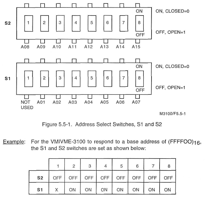
The VMEbus interface of VMIVME-3100 includes the logic required to connect the slave board to VMEbus and perform memory mapping in the VMEbus short I/O address space. In the write cycle of the board address, bits A01 to A15 are compared with the previously selected board address, which is selected by the DIP switch. If the address matches, a board selection signal is generated, which, together with the control signal received on the board, gates the data (DO to D15) to the CSR on VMIVME-3100.
The circuit requires+5V,+15V, and -15V voltages, with+5V provided to the board through P1 and P2 connectors. The onboard DC-DC converter generates+15V and -15V for the analog circuit.
Programming related
Overview
The ADC board performs memory mapping in the VME short I/O address space, occupying only one word position within the 65535 byte VME short I/O address space. The board address is selected by DIP switches, and the short I/O space is mapped from FF0000 (hexadecimal) to FFFFF (hexadecimal). The ADC data register containing 12 bit converted digital data is a read-only register, while the control status register (CSR) is a read-write register used for board control. Since these two registers use the same address, CSR access and ADC conversion end register access are selected through data bit D15.
Description of Control Status Register (CSR)
The operating mode of the CSR programming selection board, CSR is a 16 bit read-write register. To initiate AD conversion, it is necessary to set data bit D6 in CSR and program data bits DO to D5 and D8 to D14 according to the desired operating mode. Data bit D15 is used to distinguish between two possible read cycles. Writing "0" to CSR can read the converted digital data from the ADC data register, while writing "1" can read CSR.
ADC board reads data format
To read 12 bit converted data, it is necessary to first write the low-level data bit D15 into CSR. The data is only valid when data bit D15 is read as logical '0', and the valid data is included in data bits DO to D11.
Programming Example
Provides various MC68000 assembly language programming examples, including ADC conversion of P3 connector input and using AMXbus ™ Expansion of functions, testing and programming of ADC board, testing of analog output of VMIVME-4100 DAC board using ADC board, and verification of VMIVM-3200 multiplexer board in combination with VMIVME-4100 DAC board.
Configuration and Installation
Unboxing program
Some components are sensitive to electrostatic discharge, and unused boards should be stored in their original packaging. When placing the board on the workbench, it is recommended to insert conductive material underneath the board to provide conductive diversion. After receiving the goods, it is necessary to carefully inspect for any transportation damage. If there is any damage, a claim should be made to the carrier and a complete report should be sent to VMIC.
Physical installation
When installing or disassembling the board, the power should be turned off. Insert the board into the corresponding slot of the chassis, ensure correct alignment and orientation, and smoothly slide the card forward against the mating connector until it is firmly inserted.
Pre installation checklist
Before installation, it is necessary to confirm that the relevant theoretical and programming content has been read and applied. Check whether the jumper and board address switch settings installed by the factory meet the requirements, change the relevant settings as needed, confirm that the cable connection is correct, and calibrate by the factory. If recalibration is required, please refer to the relevant sections.
Board address selection switch
There are two address DIP switches on VMIVME-3100, each corresponding to an address bit or unused. When the switch is turned on, the corresponding address bit is compared with the logic "0". During the reading and writing of the DAC board, all corresponding address bits must be compared with the switch position.
Other configurations
Address modifier response selection: The response method of the address modifier code on the board can be selected through jumper wires.
ADC output encoding selection: Factory configured for straight binary digital encoding with unipolar input and offset binary encoding with bipolar input, which can be changed to binary complement code through jumper wires.
Analog input full-scale range selection: Select the full-scale range to be digitized by the ADC through jumper (JC) and related gain resistor (R28).
RDELAY (optional) selection: The factory is configured with no RDELAY resistor, and a collection setup time of 9 μ s can be selected. Different RDELAY can be chosen as needed to obtain different collection times.
Connector Description
P1 and P2 connectors connect the VMIVME-3100 board to the VMEbus backplane. P1 contains address data and control lines, as well as all additional signals required for control data transmission and other bus functions. P2's user I/O pins are provided by AMXbus ™ Used to control external multiplexing expansion boards and test analog output boards for VMIC.
The P3 connector is a Panduit 32 pin male connector that supports 16 single ended or 8-differential analog inputs, each with an associated analog ground pin.
calibration
There are four potentiometers adjusted on the VMIVME-3100, and the factory has correctly adjusted and applied anti loosening glue. If recalibration is required, the onboard precision benchmark needs to be calibrated first, and then used to recalibrate the ADC.
Maintenance and Warranty
maintenance
The maintenance section provides information on the maintenance and upkeep of VMIC products. If the product malfunctions, users should check the software, system configuration, electrical connections, etc. User level repairs are not recommended and should contact VMIC to obtain a Return Merchandise Authorization (RMA) number. The appendix contains drawings and charts for reference.
warranty
VMIC's standard products are guaranteed to be free of material and process defects within 90 days from the date of shipment. For products that meet the warranty conditions, VMIC may choose to repair or replace them at its facilities. Customers are required to notify VMIC within a reasonable time after discovering defects. Prior to returning the product, they must contact the customer service department to obtain the call ticket number and RMA number. There are corresponding regulations on the transportation method and cost of the product. In some cases, VMIC does not assume warranty or liability, and the final determination of warranty eligibility is made by VMIC. The warranty period for replacement or repair products is the same as that of the original products.
Over warranty maintenance policy
VMIC's maintenance policy for standard products is divided into two categories: product replacement and fixed price maintenance. All product repairs require return authorization, and repair pricing can be consulted with the factory representative. Payment should be made upon delivery or within 30 days after the delivery date selected by VMIC, and shipping costs should be borne by the customer (excluding warranty repairs). VMIC's repaired products are guaranteed to be free of process and material defects for 90 days from the date of shipment to the customer, and repair rates may not apply to products that have suffered abnormal physical or electrical damage.
- OMRON
- ABB
- General Electric
- EMERSON
- Honeywell
- HIMA
- ALSTOM
- Rolls-Royce
- MOTOROLA
- Rockwell
- Siemens
- Woodward
- YOKOGAWA
- FOXBORO
- KOLLMORGEN
- MOOG
- KB
- YAMAHA
- BENDER
- TEKTRONIX
- Westinghouse
- AMAT
- AB
- XYCOM
- Yaskawa
- B&R
- Schneider
- KONGSBERG
- NI
- WATLOW
- ProSoft
- SEW
- ADVANCED
- Reliance
- TRICONEX
- METSO
- MAN
- Advantest
- STUDER
- DANAHER MOTION
- Bently
- Galil
- EATON
- MOLEX
- DEIF
- B&W
- ZYGO
- Aerotech
- DANFOSS
- Beijer
- Moxa
- Rexroth
- Johnson
- WAGO
- TOSHIBA
- BMCM
- SMC
- HITACHI
- HIRSCHMANN
- Application field
- XP POWER
- CTI
- TRICON
- STOBER
- Thinklogical
- Horner Automation
- Meggitt
- Fanuc
- Baldor
- SHINKAWA
- Other Brands
- UniOP
- KUKA
- Iba
- Beckhoff
- ADLINK
-
 Rolls Royce H1111.0204 Ship Main Controller
 -
 Basler Electric BE3-32-3AC Reverse Power Relay 9 1376 00 105
 -
 Basler Electric BE3-25-1A1N4 Synch Check Relay 9319100100
 -
 Basler Electric SR4A-2B15B3A Static Voltage Regulator
 -
 Basler Electric SR4A-2B15B3E Static Voltage Regulator
 -
 Basler Electric 9170818100 Solid State Protective Relay
 -
 Basler Electric AEC63-7 Analog Excitation Controller
 -
 Basler Electric 17483 Auxiliary Module
 -
 Basler Electric BE1-59 Over Voltage Relay
 -
 Basler Electric 21600-101 Control Module
 -
 Basler Electric KR2F Generator Voltage Regulator 9056600100
 -
 Basler BE1-CDS Current Differential System
 -
 Basler Electric CBS 212 Current Boost System 9 2650 00 100
 -
 Basler Electric IFM-150 Firing Circuit Chassis
 -
 Basler Electric BE1-60 Voltage Balance Relay C1F A1P D0C3F
 -
 Basler Electric BE1-32R Power Relay A2E D1R A0N0F
 -
Basler Electric BE1-32R Power Relay A2E D1R A0N0F
-
 Basler Electric 8650C80G01 Isolation Transducer PCB Board
 -
 ETEL EA-P2M-300-4/7.5A-0100-01 AccurET Modular 300 Servo Drive
 -
 Basler Electric 87T Transformer Differential Relay
 -
 Basler Electric BE-6868 Power Transformer 5950007559202
 -
 Basler Electric PRS250 Veri-Sync Relay 9088800102
 -
 Basler Electric SCP-250-G-60 VAR Power Factor Controller
 -
 Basler DECS-150 AVR 1NS2V1N1S Voltage Regulator
 -
 Basler UFOV 260A Under Frequency Overvoltage Module
 -
 Basler MOC2 199 Motor Operated Control – Overview and Setup
 -
 Basler BE3-49R-5K5A1 Temperature Relay – Complete Guide
 -
Basler BE 20035 001 Transformer – Technical Data and Installation
-
 Basler BE 02727 001 Transformer – Specifications and Usage
 -
 Basler BE127 Under Voltage Relay – Features and Application Guide
 -
Basler CBS377 Current Boost System – Complete Technical Guide
-
 Basler BE1-87G P/N 9170818100 Differential Relay – In-Depth Specs
 -
Basler BE1-87G Generator Differential Relay – Technical Overview
-
Basler Electric SR4A2B16 SVR Static Voltage Regulator – Complete Guide
-
 Basler Electric 9261500101 Power Supply Module
 -
 Basler Electric AEM-2020 Analog Expansion Module
 -
Basler Electric DGC-2020 Digital Genset Controller 51BRBNEAH001
-
Basler Electric BE1-59N Ground Fault Overvoltage Relay
-
 Basler Electric BE1-59N-A5E-E1L-N0S1F Neutral Overvoltage Relay
 -
Basler Electric MOC2499 Motor Operator Control Potentiometer 9072300430
-
 Basler Electric BE1-50/51M Overcurrent Relay
 -
 Basler Electric 9148100106 MOC3502 Solid State Relay 250VDC 0.25A
 -
 Basler Electric CBS 212 Current Boost System 9265000100
 -
 Basler Electric 10493002 Control Module
 -
Basler BE1-32R D3E E1R A0N1F Power Relay
-
 Basler SR8A2B15B3A Static Voltage Regulator
 -
 Basler IFM-105 Firing Circuit Chassis 9324100105
 -
Basler SR4A2B05B3A Static Voltage Regulator
-
 Basler BE151G1EB6PB0N0F Protective Relay
 -
Basler BE1-59 Electric Over Voltage Relay
-
 Basler 277 Static Programmable Powerline Carrier Channel
 -
 Basler BE1-32R D1E A1P A0N1F Power Relay
 -
Basler SR4A1B07B3A Static Voltage Regulator
-
 Basler Electric BE1-700 Digital Protective Relay
 -
Basler Electric SR8A-2B01B3A Static Voltage Regulator
-
 Basler Electric SR4A-2B01B3E Static Voltage Regulator
 -
 Basler Electric 9017709102 PC Board
 -
Basler Electric SR4A-2B01B3A Static Voltage Regulator
-
 Basler Electric PRS-250 Veri-Sync Relay
 -
 Basler Electric 9066800102 Excitation Support System
 -
Basler Electric BE1-87G Generator Differential Relay 9 1708 18 100
-
 Basler Electric 36T865-2 BE03752001 Power Supply
 -
 Basler Electric M-300 149D940G02 Power Supply
 -
 Basler Electric ACA2040-25GM 4Mp 25Fps Area Scan Camera
 -
 Basler BE1-87G-S1A-A1C-A0N0 Differential Relay
 -
Basler SR8A-2B06B3E Static Regulator SR8A2B06B3E
-
 Basler SCP-210 Frequency Controller 9095400100
 -
 Basler BE1-59-A3E-A1J-N1N3F Overvoltage Relay BE159A3EA1JN1N3F
 -
Basler 9 2011 11 100 Bracket Mounted Terminal Unit
-
Basler 9 1606 00 101 Voltage Regulator
-
 Basler CBS-377 Current Boost System 9109600102
 -
 Basler 8650C72 Exciter Control Module PCB Rev 5
 -
 Basler C2EE1PA0N1F BE1-32R Reverse Power Relay
 -
 ADLINK HPCI-14S12U - Industrial Control Backplane 12PCI Backplane PCI-14S Passive Backplane
 -
-0010.png) ADLINK PCIe-GIE74C - image acquisition card 4-CH GigE Vision PoE+ Frame Grabber
ADLINK PCIe-GIE74C - image acquisition card 4-CH GigE Vision PoE+ Frame Grabber -
-0010_1.png) ADLINK PCI-8164 - control card 4-Axis Advanced Motion Controller Board
ADLINK PCI-8164 - control card 4-Axis Advanced Motion Controller Board -
 ADLINK PCIe-U304 - 4 Port USB3 PCIe Frame Grabbers USB Screw Hole Card
 -
 ADLINK PCI-9112 - Multi-Function Data Acquisition Card DAQ Card
 -
 ADLINK PCI-7432 - 51-12013-0A50 4-CH Isolated Numérique I/O PCI Cartes Digital I/O Card
 -
 ADLINK PCA-6106P3-0C1 REV.C1 - backplane 6-Slot Passive Backplane Board
 -
 ADLINK PCI-7224 - 24-CH Opto-Isolated Digital I/O PCI Board
 -
 ADLINK CPCI-7433R(G) - Digital Input Board Rear I/O CompactPCI Card
 -
 ADLINK EBP-13E4 - 51-46703-0A30 Industrial PC Backplane Passive Backplane
 -
 ADLINK PCIE-HDV62 - Image acquisition card High Definition Video Frame Grabber
 -
 ADLINK EBP-13E4 - 51-46703-0A30 Industrial Backplane Board Passive Backplane
 -
 ADLINK 90111-B1 / CPCI-6770 - PCB CPU MODULE CompactPCI Single Board Computer
 -
 ADLINK PCI-7248 - DATA ACQUISITION PCI CARD 48-CH Parallel Digital I/O Board
 -
 ADLINK PCI-7230 - 51-12003-0a50 board PCI7230 32-CH Isolated Digital I/O Card
 -
 ADLINK PCI2A000CB - 51-20000-0B30 Multi-Function DAQ Card Baseboard
 -
 ADLINK PCI-8134-005 - 4-Axis Motion Controller Card
 -
 ADLINK PCI-7224 - 24-CH Opto-Isolated Digital I/O PCI Card
 -
 ADLINK PCI-7434 - 64-CH Isolated Digital Output Card
 -
 ADLINK PCI-8132 - motion control card 2-Axis Servo & Stepper Controller
 -
 ADLINK PCI-8134 - Motion Controller PCI Card 4-Axis Controller Board
 -
 ADLINK PCI-8164 - Motion Control Card 51-12406-0A40 4-Axis Controller
 -
 ADLINK 51-12001-0C20 - Circuit Board Data Acquisition Interface Module Hardware
 -
 ADLINK NuPR0-840 - industrial control motherboard Full-Size PICMG CPU Board
 -
 ADLINK PCI-7444 - 51-12023-0A10 card 128-CH Isolated Digital Output Board
 -
 ADLINK PCI-1612B - data acquisition card 4-Port RS-232/422/485 Serial Communication Card
 -
 ADLINK PCI-6208V 009 - 8/16-CH 16-Bit Analog Output Cards PCB-I-E-482=6BX3
 -
 ADLINK NUPRO-935A/LV - industrial control motherboard Full-Size PICMG SBC Board
 -
 ADLINK PCI-9114DG - Multi-Function DAQ Card Data Acquisition PCI Card
 -
 ADLINK ACL-7130 - Data acquisition card Isolated Digital I/O Board
 -
 ADLINK ABX-6300D-4E1-BP - board ABX6300D4E1BP Video Interface Expansion Card
 -
 ADLINK CPCI-6940 - CPCI-6940/D1539/M16-0(EA)-000E 6U CompactPCI Processor Board
 -
 ADLINK NuPRO-760 - industrial control motherboard Half-Size PICMG SBC CPU Board
 -
 ADLINK IMB-M42H (G)-0020 - industrial control motherboard LGA1155 Micro-ATX Mainboard
 -
 ADLINK RTV-24 / PCI-MP4S - 51-12519-1C30 4-Channel Real Time Video Capture Board
 -
 ADLINK PCI-8134 - 4-Axis Servo & Stepper Motion Controller Card
 -
 ADLINK MXC-6101D - V.PC000.002.ST.00 Box PC Configurable Embedded Computer
 -
.png) ADLINK PCI-8134A - 51-12421-0A10 Motion Control Card 4-Axis Controller Card
ADLINK PCI-8134A - 51-12421-0A10 Motion Control Card 4-Axis Controller Card -
 ADLINK DIN-100S / DIN-100SA1 - Technology SCSI-II TB 100-PIN Terminal Block Board
 -
.png) ADLINK DIN-812M001 / DIN812M001 - 51-14034-0A1 51140340A1 Terminal Module Breakout Interface
ADLINK DIN-812M001 / DIN812M001 - 51-14034-0A1 51140340A1 Terminal Module Breakout Interface -
_1.png) ADLINK PCI-8164 - Servo motion control 4-Axis Advanced Controller Card
ADLINK PCI-8164 - Servo motion control 4-Axis Advanced Controller Card -
 ADLINK PCIe-GIE64 - Acquisition card GigE Vision PoE+ Frame Grabber
 -
 ADLINK M-302 - Industrial control motherboard ATX PC Board Mainboard
 -
 ADLINK PCI-8134 - Motion Controller PCI Card 4-Axis Controller Board
 -
 ADLINK PCI-RTV24 - Image capture card Analog Video Frame Grabber
 -
 ADLINK PCI-8102 - Motion control card 2-Axis Servo & Stepper Controller Board
 -
 ADLINK PCI-9112 REV.B1 - Card Multi-Function Data Acquisition Card
 -
 ADLINK HSI-DI32-M-N / HSL-TB32-M-DIN - Discrete I/O MODULE Distributed Automation Module System
 -
 ADLINK PCI-7296 - IO card REV.A3 96-CH Parallel Digital I/O Card
 -
-0020.png) ADLINK DIN-814P-A4 / 814Y - terminal board Motion Control Interface Block
ADLINK DIN-814P-A4 / 814Y - terminal board Motion Control Interface Block -
 ADLINK DIN-814P-A4 - 51-14056-0A10 PCB-I-E-2736=ZA01 Screw Terminal Board Breakout
 -
 ADLINK M-322 - motherboard Industrial Control Computer Mainboard
 -
 ADLINK NUPRO-406 REV:B1 - industrial control motherboard Full-Size PICMG CPU Board
 -
 ADLINK AMP-204C - card DSP-Based 4-Axis Advanced Pulse-Train Controller
 -
 ADLINK HPCI14S REV.B1 - industrial computer baseboard 14-Slot Passive Backplane


