
TOSHIBA VF-AS3 inverter RS485 communication function
Core purpose: To achieve three major functions through RS485 bus - remote control (run/stop, frequency setting, torque adjustment), parameter reading and writing (internal parameter configuration of frequency converter), and status monitoring (output frequency/current/voltage, fault code, terminal status), supporting master-slave synchronous control between frequency converters without relying on PLC or upper computer.
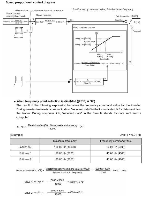
Example: Point 1 (0% → 10Hz), point 2 (100% → 80Hz), master station instruction 50% → slave station frequency=10+(50-0) × (80-10)/(100-0)=45Hz.
3. Fault handling
Main station tripping: The main station sends the command s (73H), and the slave station sets the action according to [F806]/[F826] (0=0Hz, 1=continue operation, 2=emergency stop).
Communication interruption: The communication timeout (Err5) is triggered by the slave station, and the action (such as tripping) is set according to [F824]. The master station is not affected (the status needs to be fed back through the FL fault terminal of the slave station).
Detailed explanation of communication related parameters
The communication function of the frequency converter requires the configuration of a "communication parameter group" (F8xx series), and some parameters need to be reset after power failure to take effect. The key parameters are as follows:
Parameter number, parameter name, function description, adjustment range, default value, effective method
F800/F820 RS485 baud rate setting communication rate 0=9600bps, 1=19200bps, 2=38400bps 1 (19200bps) power off reset
F801/F821 RS485 checksum setting verification method 0=no verification, 1=even verification, 2=odd verification 1 (even verification) power off reset
F802 frequency converter number setting bus address 0-247 0 immediately
F803/F823 communication timeout setting timeout detection duration 0.0 (disabled), 0.1-100.0s 0.0s immediately
F804/F824 timeout operation timeout device action 1=continue running, 4=trip immediately, 6=trip immediately after deceleration, 1=trip immediately
F806/F826 master-slave communication mode setting master-slave role master station: 3-6; Slave: 0-20 (Slave) Power off reset
F807/F827 communication protocol selection Toshiba/MODBUS 0=Toshiba protocol, 1=MODBUS-RTU 0 power-off reset
F829 RS485 (2) wiring type 2-wire/4-wire switching 0=2-wire system, 1=4-wire system 0 immediately
F830 MODBUS continuous address direct read whether to skip empty parameter 0=skip, 1=do not skip 0 immediately
F870/F871 block write parameter 1/2 setting block communication write parameter 0=disabled, 1=FA00 (run command), etc. 0 power off reset
F875-F879 block read parameters 1-5 set block communication read parameters 0=disabled, 1=FD01 (status), etc. 0 power off reset
Troubleshooting and Appendix
1. Common faults and solutions
Troubleshooting steps for possible causes of fault phenomena
Communication unresponsive 1. Baud rate/checksum/protocol mismatch; 2. Wiring error (A+/B - reversed connection, SG not connected); 3. The frequency converter number does not match; 4. Uninnected terminal/pull-up/pull-down resistor 1. Unify all device parameters (such as 19200bps+even parity+Toshiba protocol); 2. Check the A+/B - wiring to ensure SG interconnection; 3. Confirm that INV-NO is consistent with [F802]; 4. Install 120 Ω terminal resistors (at both ends) and 510 Ω pull-up and pull-down resistors (at all nodes)
Err5 tripped (communication timeout) 1. Communication cable disconnected; 2. The main station did not send data; 3. The timeout period is too short; 4. The slave station did not receive the command from the master station. 1. Check the continuity of the cable; 2. Confirm that the main station sends commands normally (such as once per second); 3. Increase [F823] (e.g. set to 1.0s); 4. Verify the master and slave station interfaces (if both are using Connector2)
Write parameter error (N0000): 1. During operation, write prohibited parameters (such as maximum frequency [FH]); 2. Parameter locking ([F700]=2/4); 3. Password setting ([F738]) 1. Write prohibition parameter after shutdown; 2. Set [F700]=0 (unlock); 3. Clear the [F738] password
Data transmission error (garbled code) 1. Electromagnetic interference (parallel wiring with the main circuit); 2. Cable over distance; 3. The terminal resistor is not connected. 1. Adjust the cable routing and keep it away from the main circuit; 2. Shorten cables or add repeaters; 3. Connect a 120 Ω terminal resistor
2. Appendix Key Information
(1) Response time calculation
Total response time=data communication time+frequency converter processing time (maximum 10ms).
Data communication time=(bytes x bits)/baud rate, bits=1 (start bit)+8 (data bit)+1 (check bit)+2 (stop bit)=12 bits (default).
Example: 19200bps, 8-byte command → communication time=(8 × 12)/19200=5ms, total response time ≈ 15ms.
(2) Corresponding Table of Inverter Models and FB05 Parameters
[FB05] The parameter is used to identify the frequency converter model, and some common models correspond to the following relationships:
Inverter model, voltage level, power FB05 (decimal), FB05 (hexadecimal)
VFAS3-2037P 200V 3.7kW 9 9
VFAS3-4055PC 400V 5.5kW 42 2A
VFAS3-4220PCE 400V(IP55) 22kW 147 93
(3) ASCII code table
Provide JIS X0201 ASCII code mapping, such as "0"=30H, "A"=41H, "d"=64H, for ASCII mode command writing and data parsing.
- OMRON
- ABB
- General Electric
- EMERSON
- Honeywell
- HIMA
- ALSTOM
- Rolls-Royce
- MOTOROLA
- Rockwell
- Siemens
- Woodward
- YOKOGAWA
- FOXBORO
- KOLLMORGEN
- MOOG
- KB
- YAMAHA
- BENDER
- TEKTRONIX
- Westinghouse
- AMAT
- AB
- XYCOM
- Yaskawa
- B&R
- Schneider
- KONGSBERG
- NI
- WATLOW
- ProSoft
- SEW
- ADVANCED
- Reliance
- TRICONEX
- METSO
- MAN
- Advantest
- STUDER
- DANAHER MOTION
- Bently
- Galil
- EATON
- MOLEX
- DEIF
- B&W
- ZYGO
- Aerotech
- DANFOSS
- Beijer
- Moxa
- Rexroth
- Johnson
- WAGO
- TOSHIBA
- BMCM
- SMC
- HITACHI
- HIRSCHMANN
- Application field
- XP POWER
- CTI
- TRICON
- STOBER
- Thinklogical
- Horner Automation
- Meggitt
- Fanuc
- Baldor
- SHINKAWA
- Other Brands
- UniOP
- KUKA
- Iba
- Beckhoff
-
 Basler BE1-25 Time Overcurrent Relay M1FA6PA4S0F
 -
 Basler SR4A2B05B3E Static Voltage Regulator
 -
 Basler DECS-200-2L Digital Excitation Control
 -
 Basler BE303280001 Control Transformer
 -
 Basler 9262103004 Voltage Regulator Board For Basler DECS-400
 -
 Basler ICRM-7 Inrush Current Reduction Module
 -
 Basler BE1-32R Power Relay
 -
 BASLER ELECTRIC KR4F VOLTAGE REGULATOR 9042600100 600V 50/60Hz
 -
 Basler 9222600101 Power Module
 -
 Basler SR8A-2B15B3A Static Voltage Regulator
 -
 BASLER BE1-87G G1E A1L A0N1P Generator Differential Relay w/ Reactor 9170818100
 -
Basler 9284900101 DECS Power Module
-
 Basler PRS250 Veri-Sync Relay
 -
 Basler BE 12296 001 Transformer
 -
 Basler 905970-104 Rev.M Voltage Regulator
 -
Basler BE1-87T Transformer Differential Relay
-
 Basler SR8A-2B15B3A Static Voltage Regulator
 -
 Basler SR32A2B05B3E Static Voltage Regulator
 -
 Basler SR4A-2B16B3A Static Voltage Regulator
 -
 Basler SR32A-2B13B3E Static Voltage Regulator
 -
 Basler KR4F Voltage Regulator 9042600100
 -
 Basler SSR 32-12 Static Voltage Regulator 400Hz
 -
 Basler CBS 212A Current Boost System
 -
 Basler MVC236 Manual Control Module
 -
Basler UFOV Protective Module 9040000100
-
 Basler SSR 125-12 Static Voltage Regulator
 -
 Basler SR4A2B10A3E Static Voltage Regulator
 -
 Basler BE1-25 Solid State Time Overcurrent Relay
 -
 Basler MVC 232 Manual Voltage Control Module
 -
Basler PRS 250 Veri-Sync Relay
-
 Basler UFOV 260A Under Frequency Over Voltage Relay
 -
 Basler RUL2098-10GC Load Relay
 -
 Basler 9 1049 04 100 PC Board
 -
Basler 125-12 Static Voltage Regulator
-
Basler PRS 250 Veri-Sync Relay
-
Basler 9185900102 SSR 125-12 Regulator
-
Basler BE12819001 Reactor
-
 Teradyne 535-100-00 Power Supply
 -
 Basler BE1-67 Directional OC Relay
 -
 Basler PRP110 Reverse Power Relay
 -
 Basler BE30631001 Isolation Transformer
 -
 Basler DECS-200-2L Digital Excitation Control
 -
 Basler BE1-47N Voltage Phase Sequence Relay
 -
 Basler AEC63-7 Analog Excitation Controller 220-277V
 -
Basler BE1-50/51B-107 Overcurrent Relay
-
 Basler Electric BE1‑32R BE1‑E1P‑BON0F Protective Relay
 -
Basler BE1-25 Solid State Time Overcurrent Relay M1EA6PA5S1F
-
 Basler MVC 232 Manual Voltage Control Module 90 37000 103 60VAC 55VDC
 -
Basler RAL6144-16GM Racer GigE Line Scan Camera
-
Basler SSR 63-12 Static Voltage Regulator
-
 Basler BE1-51A Overcurrent Relay
 -
Basler BE1-87T Solid State Protective Relay
-
Basler SR4A2B01B3A Static Voltage Regulator
-
 Basler SSR 32-12 Static Voltage Regulator
 -
 Basler TRR00696 Transformer 1KVA 115V
 -
 Basler DECS-100-B15 AVR Replacement
 -
Basler BE1-27 Under-Voltage Relay
-
 Basler ACA2000-50GM Interface Module
 -
 Basler AEC63-7 Analog Excitation Controller
 -
Basler PRS 250 Veri-Sync Relay
-
 Basler SR4A-2B15B3A Static Voltage Regulator
 -
Basler BE1-32R Power Relay
-
Basler SR8A-2B06B3E Static Voltage Regulator
-
Basler BE1-81 O/U Frequency Relay
-
 Basler BE1-51A-K2E-W6M-B1N0F Overcurrent Relay
 -
Basler BE1-851 Overcurrent Relay G3A1S1 – 48-125V AC/DC
-
 Basler BEI-51 Overcurrent Relay – NSN 5945-01-293-2363
 -
Basler Electric L301KC Protective Relay – L301KC
-
 Basler DECS-100-B15 Automatic Voltage Regulator – Generator AVR
 -
Basler SR4A-2B15B3A Static Voltage Regulator – SR4A2B15B3A
-
Basler UF 312 Under Frequency Protective Module – 9094700100
-
Basler Electric MVC 232 Manual Control Module – 60VAC 55VDC 20A
-
Basler PRS 250 Veri-Sync Relay – Generator Synchronizing Relay
-
 Basler DECS-100-A05 Digital Regulator Review
 -
 Basler AEM-2020 Analog Expansion Module Specs
 -
 Basler DECS-100-B15 Digital Excitation Specs
 -
Basler Electric 9125600106 Regulator Component
-
Basler BE1-51A-K1E-W6M-B1N0F Overcurrent Relay
-
 Basler MVC-301 MVC 300 Excitation Controller
 -
Basler SSR 32-12 Static Voltage Regulator
-
Basler 9-2849-00-101 Control Module
-
Basler BE1-51A Overcurrent Relay
-
 Basler BE1-51/27R Overcurrent Relay
 -
 Basler BE1-51 Overcurrent Relay
 -
 Basler SR8A-2B15B3A Static Voltage Regulator
 -
 Basler BE32965001 Transformer and Timer Board
 -
 Basler 9174700100 EL200-7 Excitation Limiter
 -
 Basler BE2000E AVR Voltage Regulator
 -
Basler BE1-87G Differential Relay
-
 Basler BE21834001 Generator Control Module
 -
Basler DECS-100-B15 AVR
-
 Basler D90 96801 100 PCB Card
 -
 Basler XR2002F Voltage Regulator (110 VAC, 48-480 Hz)
 -
 Basler SR8A-2B14B3A Regulator
 -
 Basler 9561500100 Module
 -
 Basler DECS-400 BE1-11 System
 -
 Basler DECS-100-B15 Excitation Control
 -
Basler SCP 210 Frequency Controller
-
Basler SR4A-2B15B3A Static Voltage Regulator
-
Basler BE1-32R Power Relay
-
 Basler PIA2400-17GM Power Interface Adapter
 -
 Basler MVC 232 Manual Voltage Control Module
 -
Basler SSR 32-12 Static Voltage Regulator
-
Basler 5MW AVR Generator Voltage Regulator
-
 Basler VR63-4B Voltage Regulator
 -
Basler DECS-100-A05 AVR for Engine Generator
-
Basler DECS-100-B15 Automatic Voltage Regulator
-
Basler BE1-32R Directional Power Relay
-
Basler BE1-87B Differential Relay
-
 Basler UFOV 260A Protective Module
 -
 Basler 9-2614-02-100 PCB Rev M
 -
Basler DECS-100-B15 Digital AVR
-
 Basler 9284900103 PS DECS-400N
 -
 Basler D4N3H1U Intertie Protection
 -
 Basler DECS-100-B15 A15 AVR
 -
 Basler KR4F Voltage Regulator
 -
 Basler BE26434 T14 Transformer
 -
 Basler SR8A-2B15B3A Regulator
 -
 Westinghouse 774B472A12 AR Relay
 -
Basler DECS-100-B15 AVR
-
Basler XR2002F Regulator 110V
-
Basler SR125-E Static Regulator
-
Basler SSR 125-12 Regulator
-
Basler MOC2599 Motor Pot
-
 Basler BE1-DFPR Feeder Relay
 -
 Basler CBS 305 Current Boost
 -
Basler BE1-25 AutoSync
-
Basler MVC 300 Voltage Control


