Welcome to the Industrial Automation website!
Product
Article
NameDescriptionContent

GE VMIVME-3115-010 32-Channel 12-bit Analog Output Board
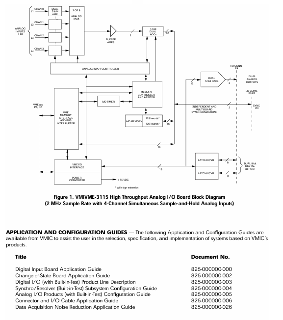
The VMIVME-3115 is a high throughput ,12-bit Analog Input/Output (AIO) board which provides four analog inputs, two analog outputs, and dual 8-bit bi-directional digital input/output ports for VMEbus system applications.
Dual-ported data memory, on-board timers, and a program-controlled bus interrupter enables the VMIVME-3115 board to support extensive analog input and output traffic with minimum involvement of the host processor.
Dual-ported data memory, on-board timers, and a program-controlled bus interrupter enables the VMIVME-3115 board to support extensive analog input and output traffic with minimum involvement of the host processor.
VMEbus Interrupt: The VMIVME-3115 can be programmed to generate an IRQ1 to IRQ7 when either buffer is full. The interrupt response vector is controlled by an on-board Interrupt Vector Register.
Board Identification: The Board Identification Register (BIR) contains the VMIVME-3115 identification code.
Transparent Operation: The following default conditions are established at RESET:
Independent continuous operation
Maximum block size (256 Kbytes)
15.625 kHz scan rate
Analog outputs off
Digital ports as inputs
VMEbus Compliance: Complies with the VMEbus Specification Rev. C.1
A32/A24/A16:D16/D08 (EO) DTB Slave:BLT
D16 Slave
Interrupter I(1) to I(7) ROAK (DYN)
Interrupt Vector: D08 (O) (DYN)
6U form factor
Interrupt Event: Either buffer full

ELECTRICAL SPECIFICATIONS AT 25 °C
Analog Inputs:
Number of Input Channels: Four differential channels; jumper-selectable
Converter Channels: Two Sample-and-Hold Amplifiers: Eight (two per input channel)
Resolution: 12 bits
Voltage Ranges: 0 to +5 V, ±5 V (options X-0-X and X-2-X), or 0 to +10 V, ±10 V (options X-1-X and X-3-X)
Input Sampling: Simultaneous sampling of all analog inputs
Interchannel Phase Skew: Less than 0.1°at 20 kHz
Scan Rate(1): Program controlled from 15.625 kCPS to 2 MCPS. See the Ordering Information.
Acquisition Time: Same as conversion cycle. .
Conversion Cycle (Settling Plus Conversion):1 m sec x 2,000,000/SCAN RATE. See Note 3.
Data Coding: Two’s complement, binary or offset binary
Gain Error: ±0.05 percent maximum
Input Offset: ±5 mV maximum
Input Impedance: 4 kW, differential; 8 kWwith 10 V input options
Input Protection: ±25 V; ±40 V with 10 V input options
Maximum Sampling Rate: 1.0 MCPS (2 channels) or 0.5 MCPS (4 channels), jumper-selectable
Common-Mode Rejection: 72 dB at 1 kHz; differential mode
Common-Mode Range: ±10 V (options X-0-X and X-2-X)±20 V (options X-1-X and X-3-X)
Crosstalk Rejection: 72 dB at 1 kHz
Analog Outputs:
Number of Output Channels: Two independent analog outputs
Resolution: 12 bits
Monotonicity: 12 bits, over operating temperature range
Output Modes: On-line (outputs connected to I/O connector) or off-line (outputs disconnected from I/O connector)
Voltage Ranges: 0 to +10 V, ± 5 V, ± 10 V, jumper-selectable
Output Impedance: Less than 0.5 W
Data Coding: Two’s complement, binary, or offset binary
Settling Time: 25 ms maximum, to 0.02 percent
Linearity Error: ±0.03 percent maximum
Output Offset: ±5 mV maximum
Load Current: ±10 mA maximum, over full output range of ±10 V
Load Capacitance: 5,000 pFd, no oscillation
Output Protection: Continuous short to ground; ±25 V for one second
Off-line Output Leakage: 50 nA maximum
1.MCPS = Million Channels per Second; kCPS = /Thousand Channels per Second
2. Each input is “pipelined” with two Sample-and-Hold amplifiers. Sample acquisition occurs while the previously acquired sample is digitized.
3.An effective conversion cycle of 500 ns (2 MCPS) is obtained by digitizing two channels simultaneously
- OMRON
- ABB
- General Electric
- EMERSON
- Honeywell
- HIMA
- ALSTOM
- Rolls-Royce
- MOTOROLA
- Rockwell
- Siemens
- Woodward
- YOKOGAWA
- FOXBORO
- KOLLMORGEN
- MOOG
- KB
- YAMAHA
- BENDER
- TEKTRONIX
- Westinghouse
- AMAT
- AB
- XYCOM
- Yaskawa
- B&R
- Schneider
- KONGSBERG
- NI
- WATLOW
- ProSoft
- SEW
- ADVANCED
- Reliance
- TRICONEX
- METSO
- MAN
- Advantest
- STUDER
- DANAHER MOTION
- Bently
- Galil
- EATON
- MOLEX
- DEIF
- B&W
- ZYGO
- Aerotech
- DANFOSS
- Beijer
- Moxa
- Rexroth
- Johnson
- WAGO
- TOSHIBA
- BMCM
- SMC
- HITACHI
- HIRSCHMANN
- Application field
- XP POWER
- CTI
- TRICON
- STOBER
- Thinklogical
- Horner Automation
- Meggitt
- Fanuc
- Baldor
- SHINKAWA
- Other Brands
- UniOP
- KUKA
- Iba
- Beckhoff
66
-
 Basler D90 96801 100 PCB Card
 -
 Basler XR2002F Voltage Regulator (110 VAC, 48-480 Hz)
 -
 Basler SR8A-2B14B3A Regulator
 -
 Basler 9561500100 Module
 -
 Basler DECS-400 BE1-11 System
 -
 Basler DECS-100-B15 Excitation Control
 -
 Basler SCP 210 Frequency Controller
 -
 Basler SR4A-2B15B3A Static Voltage Regulator
 -
 Basler BE1-32R Power Relay
 -
 Basler PIA2400-17GM Power Interface Adapter
 -
 Basler MVC 232 Manual Voltage Control Module
 -
 Basler SSR 32-12 Static Voltage Regulator
 -
 Basler 5MW AVR Generator Voltage Regulator
 -
 Basler VR63-4B Voltage Regulator
 -
 Basler DECS-100-A05 AVR for Engine Generator
 -
 Basler DECS-100-B15 Automatic Voltage Regulator
 -
 Basler BE1-32R Directional Power Relay
 -
 Basler BE1-87B Differential Relay
 -
 Basler UFOV 260A Protective Module
 -
 Basler 9-2614-02-100 PCB Rev M
 -
Basler DECS-100-B15 Digital AVR
-
 Basler 9284900103 PS DECS-400N
 -
 Basler D4N3H1U Intertie Protection
 -
 Basler DECS-100-B15 A15 AVR
 -
 Basler KR4F Voltage Regulator
 -
 Basler BE26434 T14 Transformer
 -
 Basler SR8A-2B15B3A Regulator
 -
 Westinghouse 774B472A12 AR Relay
 -
Basler DECS-100-B15 AVR
-
Basler XR2002F Regulator 110V
-
Basler SR125-E Static Regulator
-
 Basler SSR 125-12 Regulator
 -
 Basler MOC2599 Motor Pot
 -
 Basler BE1-DFPR Feeder Relay
 -
 Basler CBS 305 Current Boost
 -
 Basler BE1-25 AutoSync
 -
 Basler MVC 300 Voltage Control
 -
 Basler BE3-25A AutoSync
 -
 Basler KR7FF Static Regulator
 -
 Basler 90-49000-100 Regulator
 -
 Basler 880 kVA Dry Type Transformer Specs
 -
 Basler Electric BE1-25 Sync-Check Relay Specs
 -
 Basler SSR 125-12 Voltage Regulator Specs
 -
 Basler Electric BE1-851 Overcurrent Relay Review
 -
Basler Electric 149D930G02 Control Sub-Assembly
-
 Basler Electric BE1-81O/UT Frequency Relay Specs
 -
 Basler Electric BE1-51/27C Overcurrent Relay
 -
 Basler Electric 149D956G02 Industrial Component
 -
Basler Electric BE1-51A Overcurrent Relay Specs
-
 Basler Electric BE1-40Q Loss of Excitation Relay
 -
 Basler DECS-200 Excitation Control System
 -
 Basler DECS-200 Voltage Regulator 56-277V AC / 125V DC
 -
Basler BE1-87T Transformer Differential Relay
-
 Basler RDP-110-S1 Protection Relay
 -
 Basler BE1-700V Digital Protective Relay
 -
 Basler BE1-951 Overcurrent Protection System
 -
 Basler DECS-300 Digital Excitation Control
 -
 Basler DECS-200 Digital Excitation Control
 -
 Basler DECS-200-1C Excitation Control System
 -
Basler DECS-200-1L Digital Excitation Control
-
 Basler Electric BE1-GPS Generator Protection System
 -
Basler Electric DECS-200-1C Digital Excitation Controller
-
 Basler Electric DECS125-15 Excitation Control with Power Module
 -
 Basler Electric BE1-87G Differential Relay
 -
 Basler Electric BE1-11 Protection System I5A3M2P2N0EA00
 -
Basler Electric DECS-200-1C Excitation Control System
-
Basler Electric BE1-11g Generator Protection Relay
-
Basler Electric DECS 125-15-B2C1 V2.0.9 Excitation Control
-
 Basler Electric BE1-81O/UT3ED1JA7N2F Frequency Relay
 -
Basler Electric BE1-81O/UT3EE1YB7N1F Frequency Relay
-
 Basler Electric DECS-200-1L Digital Excitation Control System
 -
Basler DECS125-15-B2C1 Excitation Control
-
 Basler 9507900205 SSR Retrofit Voltage Regulator
 -
 Basler BE2000E Digital Voltage Regulator
 -
 Basler BE1-GPS Generator Protection System
 -
Basler DECS-250-CN1CN1N Digital Excitation Control
-
 Basler DGC-2020 Genset Controller
 -
 Basler BE1-81O UT3ED1LA7N0F Frequency Relay (Variant)
 -
 Basler BE1-81O UT3EE1YA9S0F Frequency Relay (Variant)
 -
Basler BE1-81O Over/Under Frequency Relay
-
Basler DECS125-15 Digital Excitation Control
-
Basler Electric BE1-951 Overcurrent Protection System
-
 Basler Electric BE1-700V Digital Protective Relay
 -
 Basler Electric APR63-5 Automatic Voltage Regulator
 -
Basler Electric BE1-851 Overcurrent Protection System
-
Basler Electric DECS-250-LN1SN1N Excitation Control
-
 Basler Electric BE1-87T Transformer Differential Relay
 -
Basler Electric DECS-200-1L Excitation Control System
-
 Basler Electric 9310300100 DECS-300 Excitation Control
 -
 Basler Electric SSE-N 125-4.5KW Shunt Exciter Regulator
 -
 Basler Electric DGC-2020HD-5NS1DNSBA Genset Controller
 -
Basler Electric BE1-81-O/UT3EE1JB7N1F Frequency Relay
-
Basler Electric BE1-81T1EE1WA0N1F Frequency Relay
-
 Basler Electric BE1-25M1EA6PN5R1F Sync-Check Relay
 -
 Basler Electric BE1-GPS Generator Protection System
 -
Basler Electric DECS-250-LN1SN1N Excitation Control Rev V
-
 Basler Electric DECS-250-CN2CN1N Excitation Control
 -
Basler Electric BE1-50/51B-207 Overcurrent Relay
-
Basler Electric DECS-300-C0N0 Excitation Control System
-
Basler Electric DECS-200 Digital Excitation Control System
-
Basler Electric DECS-250-LN1CN1N Excitation Unit
-
Basler Electric DECS-250 LN2SA1D Excitation Unit Specs
-
Basler Electric BE1-87T Transformer Relay Review
-
Basler Electric BE1-11 Protection System
-
Basler Electric BE1-GPS100-E4N1H1N Protection System
-
 Allen-Bradley 442G-MABH-R Safety Module
 -
 Beckhoff CX1030-0111 PLC Assembly Profile
 -
 FANUC IC693CPU364 PLC Module
 -
 Orange Denmark Type 200816 220 PLC Specs
 -
 OMRON C200H-SNT31 Sysmac PLC Module
 -
 Allen Bradley 20AB022A3AYNANC0 PowerFlex 70
 -
 OMRON C200HW-PCU01 Position Control Unit
 -
 ABB AO845A-eA Analog Output Module
 -
 OMRON CJ1M-CPU22 CPU Unit
 -
 Allen Bradley 100-E265ED11 Contactor
 -
 Honeywell 51304511-100 Interface Module
 -
 SOLEXY BXF3S0101N0018 Gateway Module
 -
 OMRON CJ2H-CPU65 CPU Unit
 -
 Automation Direct GS2-45P0 AC Drive
 -
 M68-2000 2-Axis Motion CNC Controller
 -
 OMRON CJ1M-CPU11 V3.0 PLC CPU Unit
 -
 OMRON CJ1W-NC413 4-Axis Positioning Controller
 -
 OMRON 3G2A3-PRO16 Programming Console HMI
 -
 Siemens 3VT8440-2AA04-2GA2 Molded Case Circuit Breaker
 -
 Siemens 3RT5045 Contactor Series
 -
 OMRON C200HS-CPU01-E SYSMAC PLC Controller
 -
 OMRON C500-NC103-E Positioning Control Unit
 -
 OMRON CJ1W-TC001 Temperature Control Unit
+86-153-9626-8993
WeChat
Contact

Whatsapp

After years of experience, it has developed into a group enterprise entity integrating equipment, industrial, chemical, petroleum equipment, electricity and other products trade and services.
XING-Automation


Product
Copyright © 2026 XING Group All Rights Reserved .