
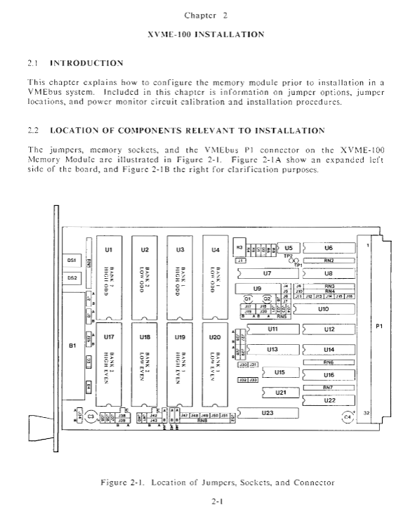
XYCOM XVME-100 memory module
(2) Environmental adaptability parameters
Specific specifications of the project, industrial scenario value
Working temperature range: 0 ° C~65 ° C (32 ° F~149 ° F), suitable for wide temperature environments such as industrial workshops and outdoor equipment cabins
Storage temperature -40 ° C~85 ° C (-40 ° F~158 ° F) to meet extreme temperature environments during storage and transportation
Humidity range of 5% to 95% RH, non condensing (requiring anti-static protection for extremely low humidity), suitable for humid environments such as high humidity workshops and coastal areas, while also indicating requirements for electrostatic protection
Vibration (working) 5~2000Hz, peak acceleration 10g, peak to peak displacement 0.025mm (maximum) to resist vibration interference during industrial equipment operation, ensuring stable module connection
Impact (working) with a peak acceleration of 30g and a duration of 11ms to withstand impacts during transportation or on-site operations, enhancing the equipment's ability to withstand harsh environments
Altitude work: 0~3048m (10000ft); Storage: 0~15240m (50000ft) suitable for special geographical environments such as high-altitude areas
Core functions and design highlights
1. Core functions of storage and configuration
(1) Dual storage group independent configuration
Configuration independence: Bank1 and Bank2 can be set completely independently through their respective jumper groups, supporting:
Different storage types (such as Bank1 caching data in RAM and Bank2 storing programs in EPROM);
Different chip capacities (e.g. Bank 1 uses 64K x 8 chips, Bank 2 uses 128K x 8 chips);
Different backup strategies (such as using battery backup for Bank1 and no backup for Bank2);
Configuration flexibility: By combining jumper wires, flexible combinations of 8 chip capacities, 4 chip speeds, 3 backup power supplies, and 2 access permissions can be achieved without the need to modify hardware or software.
(2) Multi type storage adaptation mechanism
Requirements for storage type adaptation: Key points for jumper configuration
RAM supports static RAM chips and requires low data retention current (recommended Hitachi 6264LP-15, etc.). Enable backup power (battery or+5V STDBY) and set corresponding pin definitions for jumper wires
EPROM supports 64K/128K/256K/512K/1M capacity, TTL logic level is required to disable backup power supply, and EPROM dedicated pin definition jumper is configured
Mask ROM supports 64K/128K/256K/512K capacity with EPROM configuration, no need for backup power supply
EEPROM supports 8K × 8~32K × 8 capacity and needs to support fast write/polling technology. Disable backup power and set dedicated EEPROM pins to define jumper wires
2. Data security protection mechanism
(1) Triple Data Protection Design
First layer: Under voltage protection: Built in power monitor, when the+5V voltage is lower than 4.75V, the write function of the storage chip is automatically disabled to prevent voltage fluctuations from causing data confusion; Optionally enable SYSRESET * signal to trigger system reset to protect global data;
Second layer: Backup power supply: supports on-board battery and VMEbus+5V STDBY dual backup solution, with a typical battery backup life of 6 years, suitable for independent devices without continuous power supply; +5V STDBY backup is suitable for system level backup power scenarios;
Layer 3: Physical Protection: The pin definition jumper of the storage chip can prevent hardware damage caused by accidental insertion. In case of power failure, the write path will be automatically cut off. Combined with backup power, it ensures long-term storage of RAM data.
(2) Power monitor calibration
The power monitor has been calibrated at the factory and needs to be regularly calibrated after long-term use (recommended once a year). Calibration steps:
Place the module on the expansion board, power on, and remove the J1 jumper;
Connect the negative pole of the 4.75V reference power supply to TP2 (ground) and the positive pole to the left terminal of J1;
Connect TP1 with a multimeter or oscilloscope. If the voltage is greater than 4V, rotate the POT R3 potentiometer counterclockwise until the voltage is less than 0.8V;
Slowly rotate POT R3 clockwise until the TP1 voltage jumps to a high level and stops rotating;
Remove the reference power supply and multimeter, reinstall J1, and fix the POT R3 screw with glue to prevent loosening.
3. VMEbus compatibility and interface features
(1) Bus signal compatibility
XVME-100 fully complies with the VMEbus C.1 standard, with core compatible signals including:
Address bus: A01-A23 (A24-A31 are extended addresses), supporting a 24 bit address space;
Data bus: D00-D15, supports 8-bit/16 bit data transmission;
Control signals: AS * (address gating), DS0 */DS1 * (data gating), DTACK * (data transmission confirmation), WRITE * (read-write control), etc;
Interrupt and arbitration signals: IACKIN */ACKOUT * (interrupt response daisy chain), BUS GRANT (bus grant), BUS REQ (bus request), etc.
(2) P1 connector interface definition
The P1 connector is designed with 3 rows (A/B/C) of pins, and the core pin functions are classified as follows:
- OMRON
- ABB
- General Electric
- EMERSON
- Honeywell
- HIMA
- ALSTOM
- Rolls-Royce
- MOTOROLA
- Rockwell
- Siemens
- Woodward
- YOKOGAWA
- FOXBORO
- KOLLMORGEN
- MOOG
- KB
- YAMAHA
- BENDER
- TEKTRONIX
- Westinghouse
- AMAT
- AB
- XYCOM
- Yaskawa
- B&R
- Schneider
- KONGSBERG
- NI
- WATLOW
- ProSoft
- SEW
- ADVANCED
- Reliance
- TRICONEX
- METSO
- MAN
- Advantest
- STUDER
- DANAHER MOTION
- Bently
- Galil
- EATON
- MOLEX
- DEIF
- B&W
- ZYGO
- Aerotech
- DANFOSS
- Beijer
- Moxa
- Rexroth
- Johnson
- WAGO
- TOSHIBA
- BMCM
- SMC
- HITACHI
- HIRSCHMANN
- Application field
- XP POWER
- CTI
- TRICON
- STOBER
- Thinklogical
- Horner Automation
- Meggitt
- Fanuc
- Baldor
- SHINKAWA
- Other Brands
- UniOP
- KUKA
- Iba
- Beckhoff
-
 Basler DECS-200-2L Digital Excitation Control
 -
 Basler BE1-47N Voltage Phase Sequence Relay
 -
 Basler AEC63-7 Analog Excitation Controller 220-277V
 -
 Basler BE1-50/51B-107 Overcurrent Relay
 -
 Basler Electric BE1‑32R BE1‑E1P‑BON0F Protective Relay
 -
 Basler BE1-25 Solid State Time Overcurrent Relay M1EA6PA5S1F
 -
 Basler MVC 232 Manual Voltage Control Module 90 37000 103 60VAC 55VDC
 -
 Basler RAL6144-16GM Racer GigE Line Scan Camera
 -
 Basler SSR 63-12 Static Voltage Regulator
 -
 Basler BE1-51A Overcurrent Relay
 -
 Basler BE1-87T Solid State Protective Relay
 -
 Basler SR4A2B01B3A Static Voltage Regulator
 -
 Basler SSR 32-12 Static Voltage Regulator
 -
 Basler TRR00696 Transformer 1KVA 115V
 -
 Basler DECS-100-B15 AVR Replacement
 -
Basler BE1-27 Under-Voltage Relay
-
 Basler ACA2000-50GM Interface Module
 -
 Basler AEC63-7 Analog Excitation Controller
 -
 Basler PRS 250 Veri-Sync Relay
 -
 Basler SR4A-2B15B3A Static Voltage Regulator
 -
Basler BE1-32R Power Relay
-
Basler SR8A-2B06B3E Static Voltage Regulator
-
Basler BE1-81 O/U Frequency Relay
-
 Basler BE1-51A-K2E-W6M-B1N0F Overcurrent Relay
 -
Basler BE1-851 Overcurrent Relay G3A1S1 – 48-125V AC/DC
-
 Basler BEI-51 Overcurrent Relay – NSN 5945-01-293-2363
 -
Basler Electric L301KC Protective Relay – L301KC
-
 Basler DECS-100-B15 Automatic Voltage Regulator – Generator AVR
 -
 Basler SR4A-2B15B3A Static Voltage Regulator – SR4A2B15B3A
 -
 Basler UF 312 Under Frequency Protective Module – 9094700100
 -
Basler Electric MVC 232 Manual Control Module – 60VAC 55VDC 20A
-
Basler PRS 250 Veri-Sync Relay – Generator Synchronizing Relay
-
 Basler DECS-100-A05 Digital Regulator Review
 -
 Basler AEM-2020 Analog Expansion Module Specs
 -
 Basler DECS-100-B15 Digital Excitation Specs
 -
Basler Electric 9125600106 Regulator Component
-
Basler BE1-51A-K1E-W6M-B1N0F Overcurrent Relay
-
 Basler MVC-301 MVC 300 Excitation Controller
 -
 Basler SSR 32-12 Static Voltage Regulator
 -
 Basler 9-2849-00-101 Control Module
 -
Basler BE1-51A Overcurrent Relay
-
 Basler BE1-51/27R Overcurrent Relay
 -
 Basler BE1-51 Overcurrent Relay
 -
 Basler SR8A-2B15B3A Static Voltage Regulator
 -
 Basler BE32965001 Transformer and Timer Board
 -
 Basler 9174700100 EL200-7 Excitation Limiter
 -
 Basler BE2000E AVR Voltage Regulator
 -
Basler BE1-87G Differential Relay
-
 Basler BE21834001 Generator Control Module
 -
Basler DECS-100-B15 AVR
-
 Basler D90 96801 100 PCB Card
 -
 Basler XR2002F Voltage Regulator (110 VAC, 48-480 Hz)
 -
 Basler SR8A-2B14B3A Regulator
 -
 Basler 9561500100 Module
 -
 Basler DECS-400 BE1-11 System
 -
 Basler DECS-100-B15 Excitation Control
 -
 Basler SCP 210 Frequency Controller
 -
Basler SR4A-2B15B3A Static Voltage Regulator
-
Basler BE1-32R Power Relay
-
 Basler PIA2400-17GM Power Interface Adapter
 -
 Basler MVC 232 Manual Voltage Control Module
 -
 Basler SSR 32-12 Static Voltage Regulator
 -
Basler 5MW AVR Generator Voltage Regulator
-
 Basler VR63-4B Voltage Regulator
 -
Basler DECS-100-A05 AVR for Engine Generator
-
Basler DECS-100-B15 Automatic Voltage Regulator
-
Basler BE1-32R Directional Power Relay
-
Basler BE1-87B Differential Relay
-
 Basler UFOV 260A Protective Module
 -
 Basler 9-2614-02-100 PCB Rev M
 -
Basler DECS-100-B15 Digital AVR
-
 Basler 9284900103 PS DECS-400N
 -
 Basler D4N3H1U Intertie Protection
 -
 Basler DECS-100-B15 A15 AVR
 -
 Basler KR4F Voltage Regulator
 -
 Basler BE26434 T14 Transformer
 -
 Basler SR8A-2B15B3A Regulator
 -
 Westinghouse 774B472A12 AR Relay
 -
Basler DECS-100-B15 AVR
-
Basler XR2002F Regulator 110V
-
Basler SR125-E Static Regulator
-
Basler SSR 125-12 Regulator
-
Basler MOC2599 Motor Pot
-
 Basler BE1-DFPR Feeder Relay
 -
 Basler CBS 305 Current Boost
 -
Basler BE1-25 AutoSync
-
Basler MVC 300 Voltage Control
-
 Basler BE3-25A AutoSync
 -
 Basler KR7FF Static Regulator
 -
Basler 90-49000-100 Regulator
-
 Basler 880 kVA Dry Type Transformer Specs
 -
Basler Electric BE1-25 Sync-Check Relay Specs
-
 Basler SSR 125-12 Voltage Regulator Specs
 -
 Basler Electric BE1-851 Overcurrent Relay Review
 -
Basler Electric 149D930G02 Control Sub-Assembly
-
 Basler Electric BE1-81O/UT Frequency Relay Specs
 -
 Basler Electric BE1-51/27C Overcurrent Relay
 -
 Basler Electric 149D956G02 Industrial Component
 -
Basler Electric BE1-51A Overcurrent Relay Specs
-
 Basler Electric BE1-40Q Loss of Excitation Relay
 -
Basler DECS-200 Excitation Control System
-
 Basler DECS-200 Voltage Regulator 56-277V AC / 125V DC
 -
Basler BE1-87T Transformer Differential Relay
-
 Basler RDP-110-S1 Protection Relay
 -
 Basler BE1-700V Digital Protective Relay
 -
 Basler BE1-951 Overcurrent Protection System
 -
 Basler DECS-300 Digital Excitation Control
 -
 Basler DECS-200 Digital Excitation Control
 -
 Basler DECS-200-1C Excitation Control System
 -
Basler DECS-200-1L Digital Excitation Control
-
 Basler Electric BE1-GPS Generator Protection System
 -
Basler Electric DECS-200-1C Digital Excitation Controller
-
 Basler Electric DECS125-15 Excitation Control with Power Module
 -
Basler Electric BE1-87G Differential Relay
-
 Basler Electric BE1-11 Protection System I5A3M2P2N0EA00
 -
Basler Electric DECS-200-1C Excitation Control System
-
Basler Electric BE1-11g Generator Protection Relay
-
Basler Electric DECS 125-15-B2C1 V2.0.9 Excitation Control
-
Basler Electric BE1-81O/UT3ED1JA7N2F Frequency Relay
-
Basler Electric BE1-81O/UT3EE1YB7N1F Frequency Relay
-
 Basler Electric DECS-200-1L Digital Excitation Control System
 -
Basler DECS125-15-B2C1 Excitation Control
-
 Basler 9507900205 SSR Retrofit Voltage Regulator
 -
 Basler BE2000E Digital Voltage Regulator
 -
 Basler BE1-GPS Generator Protection System
 -
Basler DECS-250-CN1CN1N Digital Excitation Control
-
 Basler DGC-2020 Genset Controller
 -
Basler BE1-81O UT3ED1LA7N0F Frequency Relay (Variant)


