
XYCOM XVME-100 memory module
Power pin:+5 V(A32/B32/C32)、+12V(C31)、-12V(A31)、+5V STDBY(B31)、GND( Multiple pins scattered to ground);
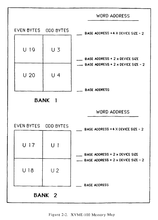
Address pins: A01-A23 (A24-A31 located in row 2B);
Data pins: D00-D07 (A1-A8), D08-D15 (C1- C8);
Control pins: AS*(A18)、DS0*(A13)、DS1*(A12)、DTACK*(A16)、WRITE*(A14) Wait.
Installation and configuration process
1. Detailed explanation of jumper configuration
XVME-100 has a total of 52 jumpers, and the core configuration items and their corresponding relationships are as follows:
(1) Address and chip size configuration (core configuration)
Configure the target jumper position configuration logic
The Bank1 base address settings for J14 (A23) and J17-J24 (A15-A22) jumper "Out" correspond to address bit 1, and "In" corresponds to address bit 0, which needs to be set according to the system address plan
Bank1 chip size setting J50-J52 8K × 8: J50=In/J51=In/J52=In;
16K×8:J50=In/J51=In/J52=Out;
32K×8:J50=In/J51=Out/J52=In;
64K×8:J50=In/J51=Out/J52=Out;
128K×8:J50=Out/J51=In/J52=In
The basic address settings for Bank2 are J16 (A23) and J26-J33 (A15-A22), which follow the same logic as Bank1. It is necessary to avoid overlapping with the address space of Bank1
Bank2 chip size setting J47-J49 with Bank1 chip size jumper logic
(2) Other key configuration jumpers
Configuration Category Jumper Position Configuration Options
Address modifier decoding Bank1: J10-J13; Bank2: J9/J12/J15 privileged access: J13 (Bank1)/J15 (Bank2) "In" is only accessed by superusers, "Out" is accessed by all users;
Data space: J11 (Bank1)/J9 (Bank2) "In" supports data access;
Program space: J10 (Bank1)/J12 (Bank2) "In" supports program access
Chip speed selection Bank1: J6-J7; Bank2:J4-J5 100ns:Out/Out; 150ns:Out/In; 200ns:In/Out; 250ns: In/In (default)
Backup power selection J34-J35 No backup: J34=A/J35=Out (default);
Battery backup: J34=B/J35=Out;
+5V STDBY backup: J34=A/J35=In
Definition of memory chip pins Bank1: J40-J46; Bank2: J2/J3/J25/J36-J39 Select according to storage type, refer to Table 2-5 in the manual for corresponding jumper combinations
2. Installation steps and specifications
(1) Preparation before installation
Environmental verification: Confirm that the installation environment temperature and humidity meet the requirements, there are no corrosive gases, and anti-static measures are in place;
Component inspection: Check that the module has no external damage, the connector pins are not bent, and the storage chip model matches the jumper configuration;
Tool preparation: Prepare anti-static wristbands, torque screwdrivers (0.5~0.8 N · m), multimeters, and chip extractors.
(2) Installation process
Chip installation:
In the power-off state, configure the corresponding jumper according to the storage type and confirm that the chip notch direction is consistent with the slot notch;
Hand hold the edge of the chip (avoid touching the pins) and insert it evenly into the 32 pin slot, ensuring that the pins are fully in contact without bending or loosening;
Rack deployment:
Confirm that the VMEbus rack power has been turned off, align the module with the guide rail, and slowly push it in until the P1 connector is fully engaged with the backplane;
Secure the front panel of the module with M3 screws and tighten to a torque of 0.5~0.8 N · m to prevent loose screws from causing poor contact;
6U panel installation (optional):
Remove the screws and handle of the original 3U panel, and transfer the handle to the XVME-945 6U panel;
Align the mounting holes of the panel and module, fix them with screws, and ensure that the panel fits snugly with the rack;
Post installation inspection:
Use a multimeter to measure the power supply voltage of the module (+5V normal, fluctuation ≤ ± 5%);
Connect the rack power supply and observe the storage group LED light (which lights up instantly during access). If there are no abnormalities, the installation is complete.
3. Common configuration examples
Example 1: Bank1 configured with 32K × 8 EPROM, base address 8E0000 Hex
Chip size jumper (Bank1): J50=In, J51=Out, J52=In;
Base address jumper (Bank1): J14=Out (A23=1), J23=In (A22=0), J21=In (A21=0), J22=In (A20=0), J24=Out (A19=1), J20=Out (A18=1), J18=Out (A17=1), J19=A (A16=0), J17=A (A15=0);
Address space: 8E0000 Hex~8FFFF Hex (a total of 128KB, i.e. 32K × 8 × 4);
Other configurations: J13=Out (all user access), J11=In (supports data access), J10=In (supports program access), J6-J7=In/In (250ns speed), J40-J46 configured according to EPROM pin definitions.
Applicable scenarios and boundary limitations
1. Core applicable scenarios
(1) Industrial automation control
Scenario features: VMEbus architecture PLC and DCS systems require stable program storage and data caching, with large environmental temperature fluctuations and vibration interference;
Recommended configuration: Bank1 uses 64K × 8 RAM to cache real-time data (battery backup), and Bank2 uses 128K × 8 EPROM to store control programs;
Core advantages: wide temperature adaptability, strong vibration resistance, reliable data backup, and support for on-site maintenance.
(2) Military embedded devices
Scenario features: VMEbus military computer, requiring resistance to harsh environments, long lifespan, low power consumption, and storage of programs and critical data;
- OMRON
- ABB
- General Electric
- EMERSON
- Honeywell
- HIMA
- ALSTOM
- Rolls-Royce
- MOTOROLA
- Rockwell
- Siemens
- Woodward
- YOKOGAWA
- FOXBORO
- KOLLMORGEN
- MOOG
- KB
- YAMAHA
- BENDER
- TEKTRONIX
- Westinghouse
- AMAT
- AB
- XYCOM
- Yaskawa
- B&R
- Schneider
- KONGSBERG
- NI
- WATLOW
- ProSoft
- SEW
- ADVANCED
- Reliance
- TRICONEX
- METSO
- MAN
- Advantest
- STUDER
- DANAHER MOTION
- Bently
- Galil
- EATON
- MOLEX
- DEIF
- B&W
- ZYGO
- Aerotech
- DANFOSS
- Beijer
- Moxa
- Rexroth
- Johnson
- WAGO
- TOSHIBA
- BMCM
- SMC
- HITACHI
- HIRSCHMANN
- Application field
- XP POWER
- CTI
- TRICON
- STOBER
- Thinklogical
- Horner Automation
- Meggitt
- Fanuc
- Baldor
- SHINKAWA
- Other Brands
- UniOP
- KUKA
- Iba
- Beckhoff
-
 Basler DECS-200-2L Digital Excitation Control
 -
 Basler BE1-47N Voltage Phase Sequence Relay
 -
 Basler AEC63-7 Analog Excitation Controller 220-277V
 -
 Basler BE1-50/51B-107 Overcurrent Relay
 -
 Basler Electric BE1‑32R BE1‑E1P‑BON0F Protective Relay
 -
 Basler BE1-25 Solid State Time Overcurrent Relay M1EA6PA5S1F
 -
 Basler MVC 232 Manual Voltage Control Module 90 37000 103 60VAC 55VDC
 -
 Basler RAL6144-16GM Racer GigE Line Scan Camera
 -
 Basler SSR 63-12 Static Voltage Regulator
 -
 Basler BE1-51A Overcurrent Relay
 -
 Basler BE1-87T Solid State Protective Relay
 -
 Basler SR4A2B01B3A Static Voltage Regulator
 -
 Basler SSR 32-12 Static Voltage Regulator
 -
 Basler TRR00696 Transformer 1KVA 115V
 -
 Basler DECS-100-B15 AVR Replacement
 -
Basler BE1-27 Under-Voltage Relay
-
 Basler ACA2000-50GM Interface Module
 -
 Basler AEC63-7 Analog Excitation Controller
 -
 Basler PRS 250 Veri-Sync Relay
 -
 Basler SR4A-2B15B3A Static Voltage Regulator
 -
Basler BE1-32R Power Relay
-
Basler SR8A-2B06B3E Static Voltage Regulator
-
Basler BE1-81 O/U Frequency Relay
-
 Basler BE1-51A-K2E-W6M-B1N0F Overcurrent Relay
 -
Basler BE1-851 Overcurrent Relay G3A1S1 – 48-125V AC/DC
-
 Basler BEI-51 Overcurrent Relay – NSN 5945-01-293-2363
 -
Basler Electric L301KC Protective Relay – L301KC
-
 Basler DECS-100-B15 Automatic Voltage Regulator – Generator AVR
 -
 Basler SR4A-2B15B3A Static Voltage Regulator – SR4A2B15B3A
 -
 Basler UF 312 Under Frequency Protective Module – 9094700100
 -
Basler Electric MVC 232 Manual Control Module – 60VAC 55VDC 20A
-
Basler PRS 250 Veri-Sync Relay – Generator Synchronizing Relay
-
 Basler DECS-100-A05 Digital Regulator Review
 -
 Basler AEM-2020 Analog Expansion Module Specs
 -
 Basler DECS-100-B15 Digital Excitation Specs
 -
Basler Electric 9125600106 Regulator Component
-
Basler BE1-51A-K1E-W6M-B1N0F Overcurrent Relay
-
 Basler MVC-301 MVC 300 Excitation Controller
 -
 Basler SSR 32-12 Static Voltage Regulator
 -
 Basler 9-2849-00-101 Control Module
 -
Basler BE1-51A Overcurrent Relay
-
 Basler BE1-51/27R Overcurrent Relay
 -
 Basler BE1-51 Overcurrent Relay
 -
 Basler SR8A-2B15B3A Static Voltage Regulator
 -
 Basler BE32965001 Transformer and Timer Board
 -
 Basler 9174700100 EL200-7 Excitation Limiter
 -
 Basler BE2000E AVR Voltage Regulator
 -
Basler BE1-87G Differential Relay
-
 Basler BE21834001 Generator Control Module
 -
Basler DECS-100-B15 AVR
-
 Basler D90 96801 100 PCB Card
 -
 Basler XR2002F Voltage Regulator (110 VAC, 48-480 Hz)
 -
 Basler SR8A-2B14B3A Regulator
 -
 Basler 9561500100 Module
 -
 Basler DECS-400 BE1-11 System
 -
 Basler DECS-100-B15 Excitation Control
 -
 Basler SCP 210 Frequency Controller
 -
Basler SR4A-2B15B3A Static Voltage Regulator
-
Basler BE1-32R Power Relay
-
 Basler PIA2400-17GM Power Interface Adapter
 -
 Basler MVC 232 Manual Voltage Control Module
 -
 Basler SSR 32-12 Static Voltage Regulator
 -
Basler 5MW AVR Generator Voltage Regulator
-
 Basler VR63-4B Voltage Regulator
 -
Basler DECS-100-A05 AVR for Engine Generator
-
Basler DECS-100-B15 Automatic Voltage Regulator
-
Basler BE1-32R Directional Power Relay
-
Basler BE1-87B Differential Relay
-
 Basler UFOV 260A Protective Module
 -
 Basler 9-2614-02-100 PCB Rev M
 -
Basler DECS-100-B15 Digital AVR
-
 Basler 9284900103 PS DECS-400N
 -
 Basler D4N3H1U Intertie Protection
 -
 Basler DECS-100-B15 A15 AVR
 -
 Basler KR4F Voltage Regulator
 -
 Basler BE26434 T14 Transformer
 -
 Basler SR8A-2B15B3A Regulator
 -
 Westinghouse 774B472A12 AR Relay
 -
Basler DECS-100-B15 AVR
-
Basler XR2002F Regulator 110V
-
Basler SR125-E Static Regulator
-
Basler SSR 125-12 Regulator
-
Basler MOC2599 Motor Pot
-
 Basler BE1-DFPR Feeder Relay
 -
 Basler CBS 305 Current Boost
 -
Basler BE1-25 AutoSync
-
Basler MVC 300 Voltage Control
-
 Basler BE3-25A AutoSync
 -
 Basler KR7FF Static Regulator
 -
Basler 90-49000-100 Regulator
-
 Basler 880 kVA Dry Type Transformer Specs
 -
Basler Electric BE1-25 Sync-Check Relay Specs
-
 Basler SSR 125-12 Voltage Regulator Specs
 -
 Basler Electric BE1-851 Overcurrent Relay Review
 -
Basler Electric 149D930G02 Control Sub-Assembly
-
 Basler Electric BE1-81O/UT Frequency Relay Specs
 -
 Basler Electric BE1-51/27C Overcurrent Relay
 -
 Basler Electric 149D956G02 Industrial Component
 -
Basler Electric BE1-51A Overcurrent Relay Specs
-
 Basler Electric BE1-40Q Loss of Excitation Relay
 -
Basler DECS-200 Excitation Control System
-
 Basler DECS-200 Voltage Regulator 56-277V AC / 125V DC
 -
Basler BE1-87T Transformer Differential Relay
-
 Basler RDP-110-S1 Protection Relay
 -
 Basler BE1-700V Digital Protective Relay
 -
 Basler BE1-951 Overcurrent Protection System
 -
 Basler DECS-300 Digital Excitation Control
 -
 Basler DECS-200 Digital Excitation Control
 -
 Basler DECS-200-1C Excitation Control System
 -
Basler DECS-200-1L Digital Excitation Control
-
 Basler Electric BE1-GPS Generator Protection System
 -
Basler Electric DECS-200-1C Digital Excitation Controller
-
 Basler Electric DECS125-15 Excitation Control with Power Module
 -
Basler Electric BE1-87G Differential Relay
-
 Basler Electric BE1-11 Protection System I5A3M2P2N0EA00
 -
Basler Electric DECS-200-1C Excitation Control System
-
Basler Electric BE1-11g Generator Protection Relay
-
Basler Electric DECS 125-15-B2C1 V2.0.9 Excitation Control
-
Basler Electric BE1-81O/UT3ED1JA7N2F Frequency Relay
-
Basler Electric BE1-81O/UT3EE1YB7N1F Frequency Relay
-
 Basler Electric DECS-200-1L Digital Excitation Control System
 -
Basler DECS125-15-B2C1 Excitation Control
-
 Basler 9507900205 SSR Retrofit Voltage Regulator
 -
 Basler BE2000E Digital Voltage Regulator
 -
 Basler BE1-GPS Generator Protection System
 -
Basler DECS-250-CN1CN1N Digital Excitation Control
-
 Basler DGC-2020 Genset Controller
 -
Basler BE1-81O UT3ED1LA7N0F Frequency Relay (Variant)


