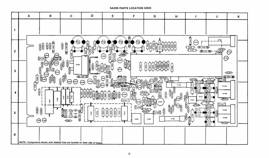
TEKTRONIX 5A22N Differential Amplifier
Core features:
Bandwidth: Maximum DC to 1MHz, bandwidth can be limited by HF-3dB (high frequency) and LF-3dB (low frequency) switches to improve signal-to-noise ratio;
Deflection coefficient: The knob skirt edge emits light and displays, supporting automatic scaling of 10X encoding probes;
Other: High common mode rejection ratio (CMRR), variable DC offset, suitable for displaying small signals at large DC levels.
TEKTRONIX 5A22N Differential Amplifier
Operation Instructions (Section 1)
1. Instrument description
Positioning: High gain differential amplifier plug-in unit, used for 5100 series oscilloscopes, can directly couple input to achieve high sensitivity.
Core features:
Bandwidth: Maximum DC to 1MHz, bandwidth can be limited by HF-3dB (high frequency) and LF-3dB (low frequency) switches to improve signal-to-noise ratio;
Deflection coefficient: The knob skirt edge emits light and displays, supporting automatic scaling of 10X encoding probes;
Other: High common mode rejection ratio (CMRR), variable DC offset, suitable for displaying small signals at large DC levels.
2. Panel controls and interfaces (key functions)
Control/Interface Function Description
Display switch plugin working status (only valid for vertical cabin), when turned on, the knob skirt light is on
POSITION adjusts the trajectory position on the screen
HF -3dB/LF -3dB - HF -3dB: 1-3-10 sequence with 7 levels (0.1kHz-1MHz), reducing the upper bandwidth limit and improving signal-to-noise ratio
-LF-3dB: 1-10-100 sequence with 7 levels (DC-10kHz), limited to 2Hz during AC coupling; adjustable DC offset in DC OFFSET level
VOLTS/DIV - Calibration mode: 18 levels 1-2-5 sequence, 10 μ V/Div to 5V/Div (accuracy 2%)
-Variable gear: Non calibrated continuous adjustment, range extended to 12.5V/Div
DC OFFSET (COARSE/FINE) requires LF-3dB to be placed in the DC OFFSET mode to achieve display adjustment of small signals at large DC levels
STEP ATTEN DC BAL balanced input amplifier to reduce trajectory offset during VOLTS/DIV switching
Input coupling button (AC/DC/GND/PRE CHG) - AC: capacitive coupling (blocking DC); DC: direct coupling
-GND: Input ground (disconnect signal); PRE CHG: Press AC+GND to pre charge the coupling capacitor to the signal DC level
+/-Input interface BNC interface,+positive signal deflects upwards, - positive signal deflects downwards; Equipped with a 10X encoded probe ring
3. Basic operation steps
Installation and startup:
Insertion: Align the plug-in guide rail with the 5100 series module compartment (priority vertical compartment: center/left; X-Y operation can be inserted into the horizontal compartment), and the panel should be level with the oscilloscope;
Power on: Adjust the oscilloscope brightness to the lowest level → Power on → Preset time base (2ms/Div) and trigger (automatic trigger).
Initial setup:
Set PLAY to ON,+/- input coupling to DC+GND, POSITION and STEP ATTEN BAL to median, HF/LF-3dB to full bandwidth, VOLTS/DIV to 50mV/Div, and variable gear to CAL (clockwise to bottom).
Preheating and trajectory adjustment:
Preheating: Short term DC measurement for 5 minutes, long-term DC measurement for 15 minutes;
Adjust the brightness to normal, and the trajectory should be near the center of the scale. Use POSITION to move the trajectory to 2 grids below the centerline.
Example of signal measurement:
Single ended DC coupling:+input connected to 400mV peak to peak calibration signal → release+GND → display 4 grid square waves (bottom alignment step 3 reference line);
Single ended AC coupling: POSITION moves the trajectory from bottom to center → presses AC → the trajectory shifts downward by about 2 grids (to the average value);
Differential AC coupling:+/- input connected to dual input cable → - input set to AC → display straight line (common mode signal suppressed).
4. Key precautions
Input protection: The maximum voltage of the input FET gate is ± 12V (diode clamp), and the input fuse will melt when the signal source current exceeds 1/16A;
Pre charge (PRE CHG): When measuring AC signals containing DC components, first connect the AC+GND signal → wait for 1 second for charging → release GND to avoid damaging the signal source due to coupling capacitor charging current;
High impedance input: When VOLTS/DIV is in the 50mV-10 μ V range, removing the circuit board jumper can disconnect the 1M Ω ground resistor, achieving high impedance input (requiring the signal source to provide a DC path for FET gate current).
5. Electrical characteristics (core parameters)
Specific parameters of characteristics
Bandwidth (-3dB) - DC coupling: DC to ≥ 1MHz (independent of deflection coefficient)
-AC coupling: 2Hz to ≥ 1MHz
Common mode rejection ratio (CMRR) - DC coupling: 10 μ V/Div-0.1mV/Div range ≥ 100dB (DC-30kHz, 20Vp-p sine wave); 0.1V/Div-5V/Div mode ≥ 50dB (100Vp-p sine wave)
-AC coupling: ≥ 80dB at 5kHz and above, reduced to 50dB at 10Hz
DC offset range -10 μ V/Div-50mV/Div range: ± 0.5V
-100mV/Div-5V/Div mode: ± 50V
Input RC 1M Ω (± 0.1%) in parallel at approximately 47pF
Maximum input voltage DC coupling: 10V (DC+peak AC) (10 μ V-50mV range); 350V (DC+peak AC) (100mV-5V range)
-AC coupling: 350VDC+10V peak AC (10 μ V-50mV range, pre charged); 350V (DC+peak AC) (100mV-5V range)
Noise at full bandwidth (DC-1MHz) ≤ 20 μ V (25 Ω source resistance, tangent measurement)

Working principle (Section 2)
1. Overall block diagram path
Signal → Input coupling (AC/DC/GND) → Input attenuator (1X/100X, frequency compensation) → Pre amplifier (differential structure, floating ground power supply) → Low frequency limiting circuit (LF-3dB switching) → Gain switching stage (VOLTS/DIV control) → Offset generator (DC OFFSET) → Isolation stage (emitter follower) → Output amplifier (push-pull structure, POSITION adjustment) → Trigger signal amplifier (output to time base plugin, 0.25V/display panel).
- ABB
- General Electric
- EMERSON
- Honeywell
- HIMA
- ALSTOM
- Rolls-Royce
- MOTOROLA
- Rockwell
- Siemens
- Woodward
- YOKOGAWA
- FOXBORO
- KOLLMORGEN
- MOOG
- KB
- YAMAHA
- BENDER
- TEKTRONIX
- Westinghouse
- AMAT
- AB
- XYCOM
- Yaskawa
- B&R
- Schneider
- Kongsberg
- NI
- WATLOW
- ProSoft
- SEW
- ADVANCED
- Reliance
- TRICONEX
- METSO
- MAN
- Advantest
- STUDER
- KONGSBERG
- DANAHER MOTION
- Bently
- Galil
- EATON
- MOLEX
- DEIF
- B&W
- ZYGO
- Aerotech
- DANFOSS
- Beijer
- Moxa
- Rexroth
- Johnson
- WAGO
- TOSHIBA
- BMCM
- SMC
- HITACHI
- HIRSCHMANN
- Application field
- XP POWER
- CTI
- TRICON
- STOBER
- Thinklogical
- Horner Automation
- Meggitt
- Fanuc
- Baldor
- SHINKAWA
- Other Brands
- UniOP
- KUKA
- Iba


