
GE VMIVME-3125 Analog Input Board
Built in power converter and ADC power supply: The power supply for the analog circuit is provided by an onboard DC-DC converter, which converts the+5 VDC of VMEbus to a regulated ± 15 VDC. The+5 VDC logic power supply for the ADC is provided by an onboard regulator, and a separate+5 V DC-DC converter is used to provide isolated analog ground for the ADC.
Configuration and Installation
Unpacking procedure: Components may be sensitive to electrostatic discharge. When handling, the board should be placed on conductive material. After unpacking, check for any transportation damage. If there is any damage, file a claim with the carrier and report to GE.
Physical installation: Power off installation, insert the board into the appropriate slot of the chassis, ensure correct alignment and orientation, smoothly slide towards the mating connector until firmly seated.
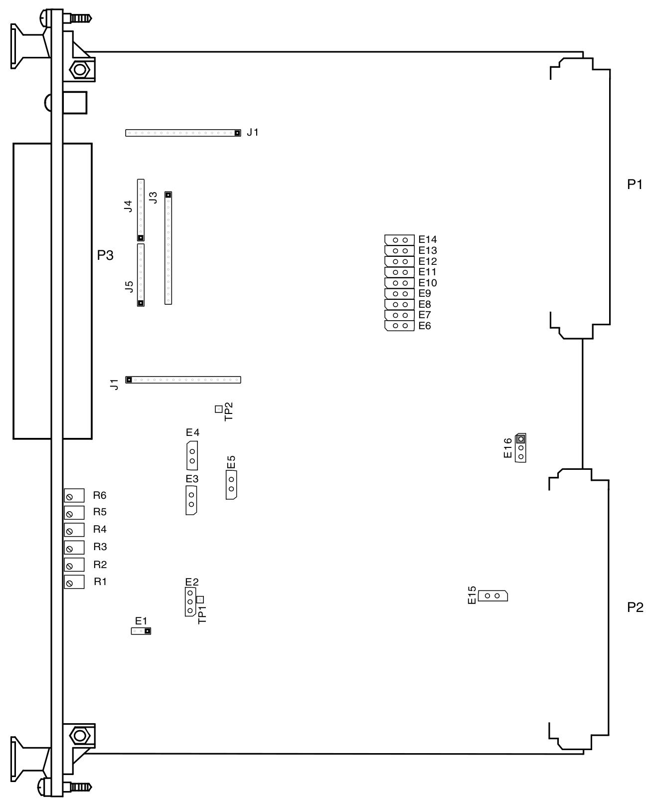
Jumper installation
Board address: occupies a short I/O address space of 128 consecutive bytes, with the base address controlled by jumper E6 to E14. The installed jumper corresponds to binary 0, and the uninstalled one corresponds to binary 1. The factory default address is short I/O $0000 (all jumper installations).
Address modifier: Jumper E16 determines the access mode of the response, including monitoring, non privileged, or both.
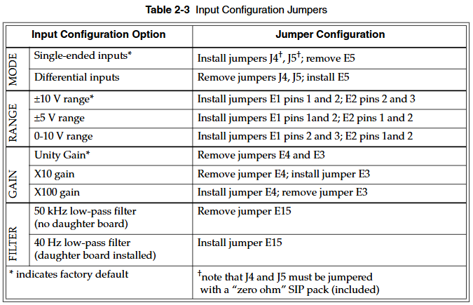
Input configuration: Three jumpers (J4, J5, and E5) are used to configure single ended or differential inputs, two jumpers (E1 and E2) control the input voltage range, two jumpers (E3 and E4) control the gain, and there are filter related jumpers. The factory default configuration is single ended, ± 10 V range, and unity gain.
Analog input connector description: 16 differential or 32 single ended analog input connections are made through the front panel 37 pin D-type connector P3, with corresponding pins and signal allocation.
Calibration Procedure: To obtain the specified accuracy of analog measurements, calibration is required for the required range and input topology. Firstly, instrument amplifier offset and BIT voltage calibration are performed, and then the corresponding offset and gain calibration procedures for the input topology are selected. Calibration requires a 5-digit digital voltmeter (DVM) and precision voltage reference equipment.
Programming
Memory mapping: occupying 128 bytes of address space, including four information and control registers, as well as a conversion data register. Depending on the jumper configuration of the board (single ended or differential input, normal or maximum buffer for differential input), there are different memory mapping tables.
Register description
Board ID register: 8-bit read-only register, offset $00, value $37, used to uniquely identify the board.
Configuration register: 8-bit read-only register, offset $01, indicating the current configuration, including input mode and filter bandwidth information.
Control/Status Register: 8-bit read/write register with an offset of $02, allowing software to control the board and indicate its current status, including functions such as stopping automatic scanning, maximum buffer, complement, mode bit, LED off, etc.
Channel pointer register: an 8-bit read-only register with an offset of $03, typically storing the input channel number currently being sampled and converted. Under specific configurations, it can determine the most recently updated data register.
Data registers: Depending on the state of the maximum buffer location, there are 16 or 32 data registers. Starting from an offset of $40, each 12 bit conversion data containing its related channel is aligned to the right within the 16 bit data register.
Built in testing function: It can test the function by applying various internal reference voltages to channel 0 input. The host software can read the value of channel 0 and compare it with the expected value. There are corresponding BIT value tables for different ranges and gain settings.
Range and gain determination: The analog gain and range can be set by the user, but the software cannot directly read these settings. It is not recommended to determine the current settings through BIT voltage stimulation, as the board must be calibrated to a single gain and range setting.
Accessing data in byte form: Data registers should typically be accessed using a single 16 bit word transfer, or two consecutive byte transfers, but there is a risk of confusion caused by data updates, which can be avoided by pausing automatic scanning or ensuring that byte accesses are continuous and undisturbed.
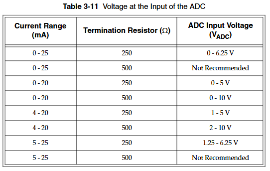
Current input options: VMIVME-3125-200 and VMIVME-3125-300 offer different terminal resistances, and the ADC input voltage is related to the current range, allowing for the calculation of the current signal through a formula.
- OMRON
- ABB
- General Electric
- EMERSON
- Honeywell
- HIMA
- ALSTOM
- Rolls-Royce
- MOTOROLA
- Rockwell
- Siemens
- Woodward
- YOKOGAWA
- FOXBORO
- KOLLMORGEN
- MOOG
- KB
- YAMAHA
- BENDER
- TEKTRONIX
- Westinghouse
- AMAT
- AB
- XYCOM
- Yaskawa
- B&R
- Schneider
- KONGSBERG
- NI
- WATLOW
- ProSoft
- SEW
- ADVANCED
- Reliance
- TRICONEX
- METSO
- MAN
- Advantest
- STUDER
- DANAHER MOTION
- Bently
- Galil
- EATON
- MOLEX
- DEIF
- B&W
- ZYGO
- Aerotech
- DANFOSS
- Beijer
- Moxa
- Rexroth
- Johnson
- WAGO
- TOSHIBA
- BMCM
- SMC
- HITACHI
- HIRSCHMANN
- Application field
- XP POWER
- CTI
- TRICON
- STOBER
- Thinklogical
- Horner Automation
- Meggitt
- Fanuc
- Baldor
- SHINKAWA
- Other Brands
- UniOP
- KUKA
- Iba
- Beckhoff
- ADLINK
-
 Basler BE1-CDS Current Differential System
 -
 Basler Electric CBS 212 Current Boost System 9 2650 00 100
 -
 Basler Electric IFM-150 Firing Circuit Chassis
 -
 Basler Electric BE1-60 Voltage Balance Relay C1F A1P D0C3F
 -
 Basler Electric BE1-32R Power Relay A2E D1R A0N0F
 -
Basler Electric BE1-32R Power Relay A2E D1R A0N0F
-
 Basler Electric 8650C80G01 Isolation Transducer PCB Board
 -
 ETEL EA-P2M-300-4/7.5A-0100-01 AccurET Modular 300 Servo Drive
 -
 Basler Electric 87T Transformer Differential Relay
 -
 Basler Electric BE-6868 Power Transformer 5950007559202
 -
 Basler Electric PRS250 Veri-Sync Relay 9088800102
 -
 Basler Electric SCP-250-G-60 VAR Power Factor Controller
 -
 Basler DECS-150 AVR 1NS2V1N1S Voltage Regulator
 -
 Basler UFOV 260A Under Frequency Overvoltage Module
 -
 Basler MOC2 199 Motor Operated Control – Overview and Setup
 -
 Basler BE3-49R-5K5A1 Temperature Relay – Complete Guide
 -
Basler BE 20035 001 Transformer – Technical Data and Installation
-
 Basler BE 02727 001 Transformer – Specifications and Usage
 -
 Basler BE127 Under Voltage Relay – Features and Application Guide
 -
 Basler CBS377 Current Boost System – Complete Technical Guide
 -
 Basler BE1-87G P/N 9170818100 Differential Relay – In-Depth Specs
 -
Basler BE1-87G Generator Differential Relay – Technical Overview
-
 Basler Electric SR4A2B16 SVR Static Voltage Regulator – Complete Guide
 -
 Basler Electric 9261500101 Power Supply Module
 -
 Basler Electric AEM-2020 Analog Expansion Module
 -
Basler Electric DGC-2020 Digital Genset Controller 51BRBNEAH001
-
 Basler Electric BE1-59N Ground Fault Overvoltage Relay
 -
 Basler Electric BE1-59N-A5E-E1L-N0S1F Neutral Overvoltage Relay
 -
Basler Electric MOC2499 Motor Operator Control Potentiometer 9072300430
-
 Basler Electric BE1-50/51M Overcurrent Relay
 -
 Basler Electric 9148100106 MOC3502 Solid State Relay 250VDC 0.25A
 -
 Basler Electric CBS 212 Current Boost System 9265000100
 -
 Basler Electric 10493002 Control Module
 -
Basler BE1-32R D3E E1R A0N1F Power Relay
-
 Basler SR8A2B15B3A Static Voltage Regulator
 -
 Basler IFM-105 Firing Circuit Chassis 9324100105
 -
 Basler SR4A2B05B3A Static Voltage Regulator
 -
 Basler BE151G1EB6PB0N0F Protective Relay
 -
Basler BE1-59 Electric Over Voltage Relay
-
 Basler 277 Static Programmable Powerline Carrier Channel
 -
 Basler BE1-32R D1E A1P A0N1F Power Relay
 -
Basler SR4A1B07B3A Static Voltage Regulator
-
 Basler Electric BE1-700 Digital Protective Relay
 -
Basler Electric SR8A-2B01B3A Static Voltage Regulator
-
 Basler Electric SR4A-2B01B3E Static Voltage Regulator
 -
 Basler Electric 9017709102 PC Board
 -
Basler Electric SR4A-2B01B3A Static Voltage Regulator
-
 Basler Electric PRS-250 Veri-Sync Relay
 -
 Basler Electric 9066800102 Excitation Support System
 -
Basler Electric BE1-87G Generator Differential Relay 9 1708 18 100
-
 Basler Electric 36T865-2 BE03752001 Power Supply
 -
 Basler Electric M-300 149D940G02 Power Supply
 -
 Basler Electric ACA2040-25GM 4Mp 25Fps Area Scan Camera
 -
 Basler BE1-87G-S1A-A1C-A0N0 Differential Relay
 -
Basler SR8A-2B06B3E Static Regulator SR8A2B06B3E
-
 Basler SCP-210 Frequency Controller 9095400100
 -
 Basler BE1-59-A3E-A1J-N1N3F Overvoltage Relay BE159A3EA1JN1N3F
 -
Basler 9 2011 11 100 Bracket Mounted Terminal Unit
-
Basler 9 1606 00 101 Voltage Regulator
-
 Basler CBS-377 Current Boost System 9109600102
 -
 Basler 8650C72 Exciter Control Module PCB Rev 5
 -
 Basler C2EE1PA0N1F BE1-32R Reverse Power Relay
 -
 ADLINK HPCI-14S12U - Industrial Control Backplane 12PCI Backplane PCI-14S Passive Backplane
 -
-0010.png) ADLINK PCIe-GIE74C - image acquisition card 4-CH GigE Vision PoE+ Frame Grabber
ADLINK PCIe-GIE74C - image acquisition card 4-CH GigE Vision PoE+ Frame Grabber -
-0010_1.png) ADLINK PCI-8164 - control card 4-Axis Advanced Motion Controller Board
ADLINK PCI-8164 - control card 4-Axis Advanced Motion Controller Board -
 ADLINK PCIe-U304 - 4 Port USB3 PCIe Frame Grabbers USB Screw Hole Card
 -
 ADLINK PCI-9112 - Multi-Function Data Acquisition Card DAQ Card
 -
 ADLINK PCI-7432 - 51-12013-0A50 4-CH Isolated Numérique I/O PCI Cartes Digital I/O Card
 -
 ADLINK PCA-6106P3-0C1 REV.C1 - backplane 6-Slot Passive Backplane Board
 -
 ADLINK PCI-7224 - 24-CH Opto-Isolated Digital I/O PCI Board
 -
 ADLINK CPCI-7433R(G) - Digital Input Board Rear I/O CompactPCI Card
 -
 ADLINK EBP-13E4 - 51-46703-0A30 Industrial PC Backplane Passive Backplane
 -
 ADLINK PCIE-HDV62 - Image acquisition card High Definition Video Frame Grabber
 -
 ADLINK EBP-13E4 - 51-46703-0A30 Industrial Backplane Board Passive Backplane
 -
 ADLINK 90111-B1 / CPCI-6770 - PCB CPU MODULE CompactPCI Single Board Computer
 -
 ADLINK PCI-7248 - DATA ACQUISITION PCI CARD 48-CH Parallel Digital I/O Board
 -
 ADLINK PCI-7230 - 51-12003-0a50 board PCI7230 32-CH Isolated Digital I/O Card
 -
 ADLINK PCI2A000CB - 51-20000-0B30 Multi-Function DAQ Card Baseboard
 -
 ADLINK PCI-8134-005 - 4-Axis Motion Controller Card
 -
 ADLINK PCI-7224 - 24-CH Opto-Isolated Digital I/O PCI Card
 -
 ADLINK PCI-7434 - 64-CH Isolated Digital Output Card
 -
 ADLINK PCI-8132 - motion control card 2-Axis Servo & Stepper Controller
 -
 ADLINK PCI-8134 - Motion Controller PCI Card 4-Axis Controller Board
 -
 ADLINK PCI-8164 - Motion Control Card 51-12406-0A40 4-Axis Controller
 -
 ADLINK 51-12001-0C20 - Circuit Board Data Acquisition Interface Module Hardware
 -
 ADLINK NuPR0-840 - industrial control motherboard Full-Size PICMG CPU Board
 -
 ADLINK PCI-7444 - 51-12023-0A10 card 128-CH Isolated Digital Output Board
 -
 ADLINK PCI-1612B - data acquisition card 4-Port RS-232/422/485 Serial Communication Card
 -
 ADLINK PCI-6208V 009 - 8/16-CH 16-Bit Analog Output Cards PCB-I-E-482=6BX3
 -
 ADLINK NUPRO-935A/LV - industrial control motherboard Full-Size PICMG SBC Board
 -
 ADLINK PCI-9114DG - Multi-Function DAQ Card Data Acquisition PCI Card
 -
 ADLINK ACL-7130 - Data acquisition card Isolated Digital I/O Board
 -
 ADLINK ABX-6300D-4E1-BP - board ABX6300D4E1BP Video Interface Expansion Card
 -
 ADLINK CPCI-6940 - CPCI-6940/D1539/M16-0(EA)-000E 6U CompactPCI Processor Board
 -
 ADLINK NuPRO-760 - industrial control motherboard Half-Size PICMG SBC CPU Board
 -
 ADLINK IMB-M42H (G)-0020 - industrial control motherboard LGA1155 Micro-ATX Mainboard
 -
 ADLINK RTV-24 / PCI-MP4S - 51-12519-1C30 4-Channel Real Time Video Capture Board
 -
 ADLINK PCI-8134 - 4-Axis Servo & Stepper Motion Controller Card
 -
 ADLINK MXC-6101D - V.PC000.002.ST.00 Box PC Configurable Embedded Computer
 -
.png) ADLINK PCI-8134A - 51-12421-0A10 Motion Control Card 4-Axis Controller Card
ADLINK PCI-8134A - 51-12421-0A10 Motion Control Card 4-Axis Controller Card -
 ADLINK DIN-100S / DIN-100SA1 - Technology SCSI-II TB 100-PIN Terminal Block Board
 -
.png) ADLINK DIN-812M001 / DIN812M001 - 51-14034-0A1 51140340A1 Terminal Module Breakout Interface
ADLINK DIN-812M001 / DIN812M001 - 51-14034-0A1 51140340A1 Terminal Module Breakout Interface -
_1.png) ADLINK PCI-8164 - Servo motion control 4-Axis Advanced Controller Card
ADLINK PCI-8164 - Servo motion control 4-Axis Advanced Controller Card -
 ADLINK PCIe-GIE64 - Acquisition card GigE Vision PoE+ Frame Grabber
 -
 ADLINK M-302 - Industrial control motherboard ATX PC Board Mainboard
 -
 ADLINK PCI-8134 - Motion Controller PCI Card 4-Axis Controller Board
 -
 ADLINK PCI-RTV24 - Image capture card Analog Video Frame Grabber
 -
 ADLINK PCI-8102 - Motion control card 2-Axis Servo & Stepper Controller Board
 -
 ADLINK PCI-9112 REV.B1 - Card Multi-Function Data Acquisition Card
 -
 ADLINK HSI-DI32-M-N / HSL-TB32-M-DIN - Discrete I/O MODULE Distributed Automation Module System
 -
 ADLINK PCI-7296 - IO card REV.A3 96-CH Parallel Digital I/O Card
 -
-0020.png) ADLINK DIN-814P-A4 / 814Y - terminal board Motion Control Interface Block
ADLINK DIN-814P-A4 / 814Y - terminal board Motion Control Interface Block -
 ADLINK DIN-814P-A4 - 51-14056-0A10 PCB-I-E-2736=ZA01 Screw Terminal Board Breakout
 -
 ADLINK M-322 - motherboard Industrial Control Computer Mainboard
 -
 ADLINK NUPRO-406 REV:B1 - industrial control motherboard Full-Size PICMG CPU Board
 -
 ADLINK AMP-204C - card DSP-Based 4-Axis Advanced Pulse-Train Controller
 -
 ADLINK HPCI14S REV.B1 - industrial computer baseboard 14-Slot Passive Backplane
 -
 ADLINK PCI-7250 - 8-CH Relay Output & 8-CH Isolated DI PCI Card
 -
 ADLINK EBP-13E2 - baseplate Passive Backplane Industrial Computer Chassis Board
 -
 ADLINK LPCI-3488A - PCI-GPIB card 51-12801-0A30 acquisition card IEEE-488 Interface Board
 -
 ADLINK PCI-6216V-GL - 51-12201-0C30 16-CH 16-Bit Voltage Analog Output Card
 -
 ADLINK ACL-8454 - 16-CH Isolated Digital I/O & 4-CH Counter Card
 -
 ADLINK HPCI-9S7U - backplane Passive Backplane Compatible with NuPRO-A301 852 841 842
 -
 ADLINK DAQ-2010-007 - Simultaneous-Sampling Multi-Function Data Acquisition Card
 -
 ADLINK MP-C154 - 51-64205-0A10 Motion Control Card 4-Axis Controller Board
 -
 ADLINK MXE-202/mSSD16B/WiFi-BT - Matrix Rugged I/O Platform Embedded Fanless Computer
 -
 ADLINK CM-920-R-17 - PC/104-Plus Single Board Computer Module Intel Celeron M
 -
 ADLINK PCI-7250 NSMP - 8-CH Relay Output & 8-CH Isolated DI Card


