
GE VMIVME-2128 128 bit high voltage digital output board
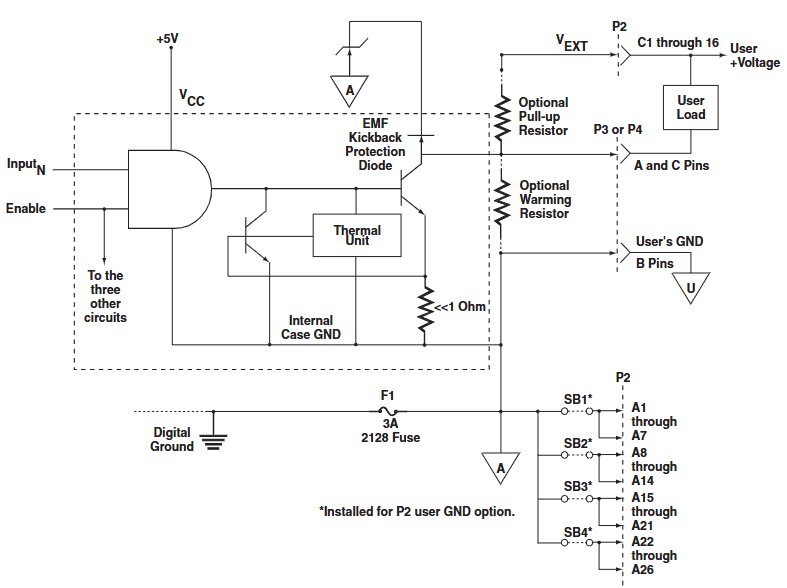
P2 user grounding option: The user grounding is connected to all B-row pins of the front panel connectors P3 and P4. If the P2 user grounding option is ordered, these grounds are also routed to pins A1 to A26 of the backplane P2 connector through the installation of short-circuit bars SB1 to SB4 (RP33 to 36). The external power supply grounding (user grounding) can now be accessed from the P2 backplane connector of the VME chassis. All 26 wires are required to provide a low resistance user load current return path. For a typical 300mA/channel load, the current of each wire can reach up to 1.48A. Each unused wire means that its current must be shared by the remaining wires, so 28 AWG or larger wires should be used.
Configuration and Installation
Unpacking procedure: Some components on GE Fanuc embedded system products may be sensitive to electrostatic discharge. When placing the board on a workbench for configuration and other operations, it is recommended to insert conductive material underneath the board to provide conductive diversion. Unused boards should be stored in their original packaging. After receiving the product, all precautions in the transport container should be followed, all items should be carefully unpacked, and a thorough inspection should be conducted for any transport damage. All claims arising from transport damage should be made to the carrier and a complete report should be sent to the GE Fanuc embedded system, requesting advice on the handling of damaged items.
Jumper and switch positions: Introduces the physical positions on the jumper, and the address modifier can change the configuration by installing the jumper at the appropriate position on connector H1, supporting multiple I/O access types. The address selection jumper is used to specify the starting board address for data transmission. The installed jumper is equal to zero, and the omitted jumper is equal to one. The factory default configuration is to respond to 0000 HEX in the short monitoring space.
I/O cable and front panel connector configuration: The output connectors (P3 and P4) on VMIVME-2128 are 96 pin DIN standard and can be used with various cables and matching connectors. Users can refer to the relevant application guide for more information. Detailed explanation of the use of user I/O pins and external voltage input for connector P2, as well as the pin configuration of output connectors for P3 and P4. The VMIVME-2128 board is designed with a high-quality ground plane, which is connected to the VME ground through fuse F1 and to the B-row pins on connectors P3 and P4 to enhance noise resistance and improve operational reliability. Users are also reminded that the grounding conductor should be connected to the power supply (GND return) associated with these signal loads, and the grounding connection should prevent excessive current (DC or noise) from flowing through the VME backplane. External user voltage should not be applied to VMIVME-2128 without connecting the VME backplane+5VDC. If these voltages cannot be applied and removed together, the preferred order is: user voltage is connected last and disconnected first.
Optional user grounding: If the user grounding option is ordered, the output return is routed to pins A1 to A26 of P2 through the installation of short-circuit bars SB1 to SB4, allowing access to the external power supply grounding from the P2 backplane of the VME chassis. It is important to maintain the grounding path resistance lower than the VME grounding path resistance and use as many wires as possible to lead out these grounding points. The current in the wires may be large, so 28 AWG or larger wires should be used, while being careful not to exceed the maximum current rating of the connector pins.
Preheating resistor: When the incandescent lamp is initially turned on, the cold filament resistor is the smallest, usually allowing 10 to 12 times the surge current. A surge current of 1A or greater will force the output driver to enter the return current limit. To avoid this problem, preheating or current limiting resistors should be used in the lamp circuit. The preheating resistor should consume about 10% of the rated (hot) current of the bulb. A ten pin SIP socket is provided on the board for preheating resistors, which must be bus type, with pin 1 as the common terminal and pin 1 of the socket grounded. The power rating of the preheating resistor should be sufficient to handle the required power consumption.
Programming
Register Mapping: VMIVME-2128 includes a 16 bit board ID register, a 16 bit CSR, and eight 16 bit ODRs, providing register address mapping. ODRs allow control of 128 high-voltage digital output channels, which can be addressed as four 32-bit long words, eight 16 bit words, or sixteen 8-bit bytes. ODRs can be read under program control for data verification or diagnostic testing. CSR and board ID can be addressed as 16 bit words or two 8-bit bytes, and ID and CSR bit mappings as well as ODR bit mappings are provided. The board uses a 32 byte address space.
Detailed programming: In output data transmission, the data register address mapping displays the correspondence between ODR (DR0 to DR7) and output data channels 127 to 0. The built-in testing function provides real-time loopback data verification and offline diagnostic execution capability. The offline built-in testing function is activated by setting the test mode (TM) bit in CSR to logic "zero". When the TM bit is set, all output drivers are in three states, and test data can be written into the selected data register and read back during read transmission without affecting the user device. When the test mode is turned off, the data can also be read back, allowing online testing of the board. The test mode bit and fault LED control bit are initialized to active state when powered on or system reset, so the fault LED lights up and the output driver is disabled. A simplified programming flowchart is also provided.
- OMRON
- ABB
- General Electric
- EMERSON
- Honeywell
- HIMA
- ALSTOM
- Rolls-Royce
- MOTOROLA
- Rockwell
- Siemens
- Woodward
- YOKOGAWA
- FOXBORO
- KOLLMORGEN
- MOOG
- KB
- YAMAHA
- BENDER
- TEKTRONIX
- Westinghouse
- AMAT
- AB
- XYCOM
- Yaskawa
- B&R
- Schneider
- KONGSBERG
- NI
- WATLOW
- ProSoft
- SEW
- ADVANCED
- Reliance
- TRICONEX
- METSO
- MAN
- Advantest
- STUDER
- DANAHER MOTION
- Bently
- Galil
- EATON
- MOLEX
- DEIF
- B&W
- ZYGO
- Aerotech
- DANFOSS
- Beijer
- Moxa
- Rexroth
- Johnson
- WAGO
- TOSHIBA
- BMCM
- SMC
- HITACHI
- HIRSCHMANN
- Application field
- XP POWER
- CTI
- TRICON
- STOBER
- Thinklogical
- Horner Automation
- Meggitt
- Fanuc
- Baldor
- SHINKAWA
- Other Brands
- UniOP
- KUKA
- Iba
-
 Honeywell 30751044-008 ROM Card
 -
 Honeywell 5SE1-12 Micro Switch Specifications
 -
 Schneider AS-BDAU-204 Analog Output Module
 -
 K93712 Expansion Kit Industrial Module
 -
 MGE DCHEN 3400116300 Circuit Board
 -
 Siemens 6SE7036-1EE85-1HA0 Rectifier Board
 -
 Renesas UPD70F3624GBA1 Microcontroller
 -
 Omron E5AC-CX4A5M-014 Temperature Controller Parameters
 -
 GE IS200TBCIH1BCE Contact Input Board
 -
 Fanuc A05B-2255-C101#EAW Teach Pendant Data
 -
 Rieter RMC186C RMC RIO-1 PLC Controller
 -
 Siemens PXC24.2-EF32.A Building Automation Controller
 -
 Fanuc A16B-1200-0220 PC Memory Board F3
 -
 Omron CJ2M-CPU33 PLC CPU Module
 -
 Beckhoff EL1918 Safety Input Terminal EtherCAT
 -
 Fanuc A16B-1212-0871 CNC PCB Board
 -
 GE Fanuc IC697BEM713J PLC Module
 -
 Mitsubishi A2ACPU-R21 PLC CPU Module
 -
 Programmable Relay 230V AC 16 Inputs 8 Outputs T2UK
 -
 Schneider F3SP71-4S Safety PLC Module
 -
 NEED-24DC- T2UK Programmable Relay 24V 16in 8out
 -
 Siemens 3RT1075-6SP36 SIRIUS Power Contactor 200kW
 -
 GE 1C31170G02 Printed Circuit Board Module 94V-0
 -
 BPT 67200020 Multifunction Touch Terminal 50Hz
 -
 Fanuc A16B-2200-0931 Option Board with Daughter Cards
 -
 Honeywell FC-SDOL-0424 I/O Module Board
 -
 Lenze EMF2179IB DeviceNet Communication Module
 -
 Yaskawa CIMR-JC4A0007BAA J1000 VFD 0.4kW
 -
 Yokogawa PSBCMNBN Bus Continuation Module ProSafe-PLC
 -
 Phoenix Contact PLC-BPT-24DC/1/SEN Solid-State Relay
 -
 Allen-Bradley 193-EC2AB E3 Plus Overload Relay
 -
 GE DS200TCTGG1AFF Turbine Control Board
 -
 Westinghouse 1C31170G02 Ovation Module
 -
 Mitsubishi A2ACPU21 Programmable Controller Review
 -
 710-95045-AD PLC I/O Operation Console Cable
 -
 Allen-Bradley 1785-L11B PLC-5 Processor Specifications
 -
 BEMAC UST-202-D 1307D V08B2 Circuit Board
 -
 Pilz 312070 PSSu H PLC1 FS Safety Module
 -
 Keyence QS-MB1 Safety Network Module Overview
 -
GE Fanuc IC693CPU372 CPU Module 90-30 Series
-
 Mitsubishi RJ71EIP91 EtherNet/IP Module
 -
 Schneider LXM62DD27D21000 Lexium 62 Servo Drive
 -
 Mitsubishi Q13UDEHCPU Universal PLC CPU Module
 -
 B&R X20CP3585 Programmable Controller X20 CPU
 -
 Siemens 6FC5203-0AF02-0AA0 Sinumerik Operator Panel
 -
 IWKA PG02 VKR TEL-Z Self-Sufficient Measuring System
 -
 Schneider BMXCPS2010 PLC Power Supply Modicon M340
 -
 Mitsubishi A171SCPU Motion Servo CPU Specifications
 -
 PLC Board with Finder 44.52 Relay Module 6A 250V
 -
 Honeywell DOP 09436601 Measurex Module Data
 -
 Fanuc A20B-8101-0320 CNC Circuit Board
 -
 KUAX 680I V.24 PLC Module 68142304
 -
 Allen Bradley 1785-L30B PLC 5/30 Processor
 -
 Phoenix ILC 191 ETH 2TX 2700976 Ethernet Controller
 -
 Siemens 6SY7000-0AC80 PLC Power Supply Module
 -
 Reliance Electric MACS 804.46.20 CWW PLC Drive
 -
 Omron CP1E-N60DR-D PLC CPU 36 Input 24 Output
 -
 Mitsubishi Melsec PLC System A2ACPU A63P AY13E AX82
 -
 Square D PAF361600DC1680 2000A Circuit Breaker
 -
 MERLIN GERIN STR 58U 5000A Electronic Trip Unit
 -
 Omron CJ1W-SCU21-V1 Serial Communication Unit
 -
 SICK S30A-6011EA S3000 Safety Laser Scanner
 -
 Mitsubishi Q00JCPU-S8 Universal Programmable Controller
 -
 Allen-Bradley 20AB9P6C3AYNANC0 PowerFlex 70 AC Drive
 -
 SYSMELEC Handheld Robot Automation Controller
 -
 LG Display LB315WRM-SVA1 32 Inch 4K LCD Panel
 -
 Mitsubishi Kakoki E Series PLC I/O Modules
 -
 Allen-Bradley 1440-VST02-01RA Dynamic Measurement Module
 -
 Beckhoff EL5042 EtherCAT Encoder Terminal
 -
 Beckhoff CX5010-0112 Embedded PC Controller
 -
 Guardmaster 440R-D22R2 Safety Relay Specifications
 -
 NL12880BC20-10ND Industrial Display Panel Data
 -
 LFI 12X5326-S1 Slide-in Control Board Technical Data
 -
 Modicon AS-9370-001 Programmable Controller Data
 -
 Mitsubishi Kakoki E-01B-4130 PLC Module Overview
 -
 Guardmaster 440R-D22S2 Dual Input Safety Relay Data
 -
 NL10276AC30-48D Industrial LCD Display Panel Data
 -
 GE ICMFA000000-ABAC Field Control Module Specification
 -
 Siemens 6SN1123-1AB00-0BA1 SIMODRIVE Module Review
 -
 Siemens 6SL3210-1SE23-2AA0 Power Module Technical Data
 -
 Schmersal T.250-11z-t Limit Switch
 -
 Schmersal T.250-11z-t Limit Switch
 -
 Honeywell 900H32-0102 ControlEdge 900 PLC
 -
 Siemens 6FX1132-1BA01 PCB B84141-A-A40
 -
 BEMAC UST-202-D 1307D PLC Circuit Board
 -
 Mitsubishi HS-MF23-S2A Servo Motor
 -
 B&R 3AI775.6 Analog Input Module
 -
 Omnipure 69003 Rev 11 3-Phase Gate Board PCB
 -
 Pilz 751134 PNOZ s4 C Safety Relay
 -
 Proface PFXGM4301TAD HMI Graphic Panel
 -
 Keyence KV-RC8BXR Programmable Controller
 -
 Siemens 6GK7243-1BX30-0XE0 CP 1243-1 Ethernet Module
 -
 Mitsubishi GT2310-VTBA GT2310-VTBD HMI 10.4 Inch
 -
 Schmersal SRB-NA-R-C.21-24V Safety Relay Module
 -
 Emotron 01-2520-40 M20 Shaft Power Monitor 3x380-500V
 -
 Omron CQM1 SYSMAC PLC System PA203 ID211 OC221
 -
 ABB CI830 3BSE013252R1 Profibus DP V1 Module
 -
 B&R 4PP035.0300-01 Power Panel PLC Module
 -
 SICK S30A-6111CL S3000 PROFINET Safety Laser Scanner
 -
 Siemens 6ES7215-1HG40-0XB0 CPU 1215C AC/DC/RLY
 -
 Automation Direct H2-ECOM100 Ethernet Module Details
 -
 Siemens 6GK1143-0TB01 CP 1430 TF Module Review
 -
 Siemens Simatic 505 10 Slot PLC Rack Technical Review
 -
 Automation Direct EZ-SP Message Display Unit
 -
 Mitsubishi A1SJ71QE71N-B5T Ethernet Interface Unit
 -
 Modicon AS-P810-000 Modbus Plus Processor Unit
 -
 Honeywell 51309241-175 TK-PPD011 PWA Specifications
 -
 Omron S8AS-24006N Smart Power Supply Specifications
 -
 Beckhoff EL3218-0018 EtherCAT Terminal Specifications
 -
 Omron CJ1W-PRT21 PROFIBUS-DP Interface Unit
 -
 Inovance AC810-0122-U0R0 PLC Controller
 -
 Cypress CY7C1021CV33-10ZXCT 1Mb SRAM IC
 -
 GE Fanuc IC695CPU315-CD PLC CPU Module RX3i
 -
 Drager 8312088 PCB Safety Module PAC 5500
 -
 Weltronic H70-T02A S430-V1.2 Weld Timer PLC
 -
 B&R 3AM051.6 PLC Analog Input Module
 -
 Schneider BMENOC0301 Communication Module M580
 -
 Mitsubishi FX3UC-32MT-LT PLC Controller
 -
 Omron TZ-1G TZ-1GV TZ-1GV2 TZ-1GV22 Motion Switch
 -
 Mitsubishi AJ71C21-B1-S2 PLC Controller 424749
 -
 Beckhoff EL5042 EtherCAT Encoder Terminal BiSS C
 -
 Eaton easyE4 Programmable Relay 12 Inputs 8 Outputs
 -
 Carel PCO5 P+ 500BAA000L0 Programmable Controller
 -
 Siemens 6ES7223-1PL22-0XA0 EM223 I/O Module 16DI 16DO
 -
 Lenze EMF2179IB DeviceNet Communication Module
 -
 Mitsubishi Q173DCPU Motion CPU Module
 -
 B&R X20AT2222 Temperature Input Module Pt100
 -
 Siemens SITOP UPS1100 Battery Module 7Ah 6EP4134-0GB00-0AY0


