GE DS200TCDAG2B Digital I/O Board
GE DS200TCDAG2B Digital I/O Board
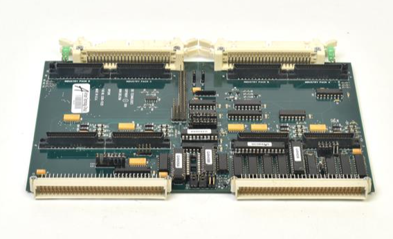
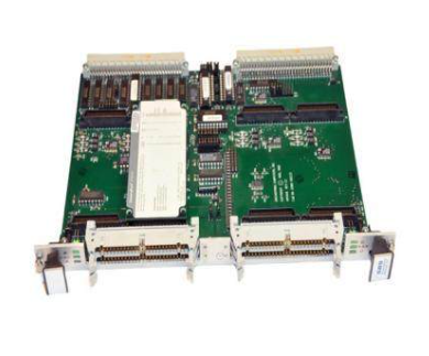
Part Number DS200TCDAG2B Manufacturer General Electric Country of Manufacture As Per GE Manufacturing Policy Series Mark V Function Module Availability In StockDS200TCDAG2B is a Digital Input/Output Board developed by GE under Mark V series. Several programmable read-only memory (PROM) modules and one microprocessor are both present on the board. Two 50-pin connectors and one block of ten LEDs are also included. 8 jumpers and 1 LED are included on it. The 50-pin connectors transfer signals to the DTBA and the DTBB boards mounted in the drive.
Ribbon cables with a plugged-in one end are connected to the 50-pin connectors. The other end of the ribbon cable attaches to either the DTBA or the DTBB boards. Take note of the 50-pin ribbon cable routing inside the drive before removing the board to replace it, and keep it the same when you replace the board. A block of 10 LEDs that are arranged in a row are present on the board. The LEDs flash sequentially from left to right when the board is powered and operating normally. As long as regular processing keeps going, the sequence will continue. The LEDs flash in a pattern to depict the error or warning code when an error or warning is encountered. All 10 LEDs are lighted at once when the board is turned on to check its operation.
The block of 10 LEDs is hidden when the board is mounted in the drive between many other boards in the board cabinet. The one green LED on the board's side, which is there to provide a rapid visual indicator of the board's condition, can be seen by the operator. TCDA Connectors JP - Distributes power from the TCPS board to the Q11, Q21, and Q51 cores, respectively, in the R1, R2, and R5 cores. JQ - Attaches to the DTBA board's JQR connector. transports the DTBA board's contact input signals to the TCDA board. JR -Attaches to the DTBB board's JRR socket. transports the DTBB board's contact input signals to the TCDA board. The TCRA board's location four is where JO1 writes the contact output (relay/solenoid) signals.
Not used in Q11 because TCQE in R1 directly controls the relays at location 4 in the Q core. The contact output (relay/solenoid) signals are written by JO2 to position 5 of the TCRA board. For the IONET signals, use JX1's shielded twisted pair. The JX2 connection on the TCEA board at position 5 of the P1 core receives the signals written by the TCDA board in the Q11 core. The signals are written to the JX connection on the CTBA terminal board in the R5 core by the TCDA board in the Q51 core. JX2 - Used for the identical purpose as JX1. JX1 or JX2 can be applied. TCDA Contact Output (Relay/Solenoid) The JO1 and JO2 connections are used to send the contact output signals to the TCRA boards.
OTHER INFORMATION
• Up to 1.26 GHz Pentium® III processor with 256 KB advanced transfer cache
• Up to 512 MB PC-133 SDRAM using a single SODIMM
• Internal AGP SVGA controller with 4 MB display cache
• 133 MHz system bus via Intel® 815E chipset
• Dual Ethernet controllers supporting 10BaseT and 100BaseTX interfaces
• Optional PCI dual channel Ultra160 SCSI
• Up to three (two with rear I/O support) PMC expansion sites (IEEE-P1386 common mezzanine card standard, 5 V)
• Up to 1 GB bootable flash on secondary IDE (optional)
• Two 16-bit and two 32-bit programmable timers
• 32 KB of nonvolatile SRAM
• Software-selectable watchdog timer with reset
• Remote Ethernet booting
• Optional IDE hard disk drive
• VME64 modes supported: A32/A24/D32/D16/D08(EO)/MBLT64/BLT32
• VMEbus interrupt handler, interrupter and system controller
• Includes real time endian conversion hardware for littleendian and big-endian data interfacing (patent no. 6,032,212)
• Enhanced bus error handling
• Passive heat sink

- User name Member Level Quantity Specification Purchase Date
- Satisfaction :
-


