SIEMENS C500 microcontroller architecture and instruction set
Condition 1 (Priority Blocking): Currently processing an interrupt of the same or higher priority.
Condition 2 (instruction completion blocking): The current instruction has not yet been executed to the last machine cycle. This ensures that the current instruction can be fully executed.
Condition 3 (Critical Instruction Blocking): The currently executing instruction is RETI (Interrupt Return), or an instruction that writes to the Interrupt Allow Register (IE) or Interrupt Priority Register (IP). The blocking will continue until the instruction is executed and another instruction is executed. This mechanism ensures that modifications to the interrupt system can take effect stably.
3. Precise calculation of interrupt response time
The interrupt response time is defined as the time interval between the time when the external interrupt request signal takes effect (the request flag is set) and the time when the first instruction of the interrupt service program starts executing.
According to the timing analysis in the manual, an interrupt requires at least 3 complete machine cycles from being detected to completing hardware LCALL (1 cycle for detecting flags and 2 cycles for executing LCALL). In the worst-case scenario, if the interrupt request encounters a blocking condition, the response time will be extended:
If blocked by condition 2 (instruction not completed), the maximum waiting time shall not exceed 3 cycles. Because the longest instruction (MUL or DIV) only requires 4 cycles, and interrupt detection occurs in the last cycle of each instruction.
If blocked by condition 3 (RETI or write IE/IP), the maximum waiting time should not exceed 5 cycles (1 cycle to complete the current RETI/write operation, plus up to 4 cycles to complete the immediately following instruction - if that instruction happens to be MUL or DIV).
Therefore, for a single interrupt system, the interrupt response time of C500 is always between 3 and 9 machine cycles. For a 12MHz crystal oscillator system (one machine cycle=1 µ s), this corresponds to a delay of 3 µ s to 9 µ s, providing highly predictable performance for hard real-time applications.
External Memory Access Timing and Bus Design
C500 accesses external program memory and data memory through standard bus interfaces, and understanding its timing is crucial for hardware design.
1. Address/data reuse
When accessing external memory, the P0 port assumes the time division multiplexing function for the low 8-bit address and 8-bit data, while the P2 port outputs the high 8-bit address (for MOVX @ DPTR or external fetch) or maintains its SFR content (for MOVX @ Ri). External address latches (such as 74HC373) use the falling edge of the ALE (Address Latch Enable) signal to latch the lower 8 bits of the address on port P0. Afterwards, the P0 port is switched to the data bus.
2. Two access modes
16 bit address access (MOVX @ DPTR): P2 port continuously outputs the content of DPH (high 8-bit address) throughout the entire access cycle. P0 port outputs DPL when ALE is valid, and then switches to data signal. This mode can access a complete address space of 64 KB.
8-bit address access (MOVX @ Ri): The P2 port maintains its existing SFR value throughout the entire cycle and does not automatically output the higher 8 bits of the address. The CPU uses the P0 port to output the content of Ri (8-bit address) and multiplex it with the data. This method is commonly used for "paging" expansion, where the P2 port is pre-set as a page address by software to enable external RAM access exceeding 256 bytes.
Important hardware precautions: During external memory access, the CPU will write FF H to the P0 port latch (SFR). Therefore, during external memory access, the software must not execute the MOV P0 instruction to modify the P0 port, otherwise it will damage the current bus cycle data. In addition, for the ROM free version (EA grounded), the entire 64 KB program space is external, and the P2 port will be fully occupied as an address line, which cannot be used for general-purpose I/O.
Instruction set: Functional classification and optimization of 111 instructions
The instruction set of C500 is fully compatible with the standard 8051, with a total of 111 instructions, including 49 single byte instructions (44%), 45 double byte instructions (41%), and 17 three byte instructions (15%). Efficient instruction encoding means that C500 can achieve higher code density at the same clock frequency.
Overview of Addressing Modes
C500 supports 5 addressing modes, each corresponding to a specific memory space, as shown in Table 2.
Table 2 Addressing Modes and Corresponding Memory Spaces
Memory space accessed in addressing mode
Address the R0-R7, ACC, B, CY bits of the currently selected register group DPTR
Directly addressing the low 128 bytes of internal RAM SFR
Immediate addressing of program memory (constant)
Register indirect addressing internal RAM (@ R0/@ R1/SP), external data storage (@ R0/@ R1/@ DPTR)
Base address register plus index addressing program memory (@ A+DPTR, @ A+PC), used for lookup tables
2. PSW impact of arithmetic operation instructions
- ABB
- General Electric
- EMERSON
- Honeywell
- HIMA
- ALSTOM
- Rolls-Royce
- MOTOROLA
- Rockwell
- Siemens
- Woodward
- YOKOGAWA
- FOXBORO
- KOLLMORGEN
- MOOG
- KB
- YAMAHA
- BENDER
- TEKTRONIX
- Westinghouse
- AMAT
- AB
- XYCOM
- Yaskawa
- B&R
- Schneider
- Kongsberg
- NI
- WATLOW
- ProSoft
- SEW
- ADVANCED
- Reliance
- TRICONEX
- METSO
- MAN
- Advantest
- STUDER
- KONGSBERG
- DANAHER MOTION
- Bently
- Galil
- EATON
- MOLEX
- DEIF
- B&W
- ZYGO
- Aerotech
- DANFOSS
- Beijer
- Moxa
- Rexroth
- Johnson
- WAGO
- TOSHIBA
- BMCM
- SMC
- HITACHI
- HIRSCHMANN
- Application field
- XP POWER
- CTI
- TRICON
- STOBER
- Thinklogical
- Horner Automation
- Meggitt
- Fanuc
- Baldor
- SHINKAWA
- Other Brands
- UniOP
- KUKA
- Iba
-
 ABB SCC-C 23070-0-10232110 gas cooler
 -
 Sick LGTN101-521 CPU Module
 -
 Okuma 1911-2836 PLC Circuit Board
 -
 Mitsubishi Melsec PM-120M PLC
 -
 Omron F210-C15 Vision Mate Controller System
 -
 Siemens 7ML5110-1GD07-4AF3 Ultrasonic Level Gauge
 -
 ABB Pluto S46 V2 Safety Relay
 -
 Omron Z3RN-5A Optical Serial Link
 -
 Omron R7D-APA3H 30W Servo Drive
 -
 Giddings Lewis 502-03638-41R3 PLC Processor
 -
 Omron SCY-P1 Sequencer Controller
 -
 Siemens C98043-A7002-L1-13 PCB Board
 -
 SACS TECNICA Palletizer PC PLC Control System
 -
 AutomationDirect T1F-14THM PLC Module T1F14THM
 -
 OMRON C200H-AD003 Analog Input Unit PLC Module
 -
 Applied Materials 0010-A0000 Electricity Box PLC 200mm
 -
 ABB RVT-6 Power Factor Controller RVT6
 -
 Allen-Bradley 2094-BC01-MP5-M Kinetix 6000 Axis Module
 -
 OMRON FQM1S-MC233 Motion Controller PLC Module
 -
 OMRON C200H-SNT31 PLC Special I-O Module
 -
 Yaskawa SGMPH-04AAA61D-OY Servo Motor 400W 200V
 -
 Yaskawa SGMGH-09DCA6F-OY AC Servo Motor 850W 400V
 -
 REFU ELEKTRONIK SR17002 PLC Logic Module Circuit Board
 -
 Siemens 6DP1231-7AA PLC Board Module Industrial Control
 -
 ABB SACE ISOMAX S3 N 160 Molded Case Circuit Breaker
 -
 OMRON C120-SC024-V1 SYSMAC C120 Compact PLC Unit
 -
 OMRON CJ1W-SCU41-V1 Serial Communication Unit PLC Module
 -
 OMRON 3G3MX2-A4110-ZV1 MX2 Variable Frequency Drive
 -
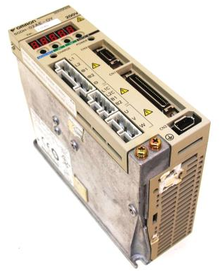
 Yaskawa SGDH-04AE-OY Sigma-II Servo Driver 400W 200V
 -
 OMRON CQM1-AD041 Analog Input Module PLC I/O Unit
 -
 Delta Omega XML2-0060-45-4/S-A Servo Drive
 -
 Omron CJ1W-AD041 Analog Input
 -
 Omron CJ1W-NC271 Position Control Unit
 -
 Omron CJ1G-CPU45H PLC CPU
 -
 Omron CJ1W-EIP21 EtherNet/IP Unit
 -
 Omron F210-C15 Vision Mate Controller
 -
 Omron CQM1H-ADB21 Analog I/O Board
 -
 Omron GRT1-PRT PROFIBUS DP-V1 Adapter
 -
 Omron CP1H-Y20DT-D PLC CPU
 -
 TE.CO TFX 4G 1.5 Grey Cable 470m
 -
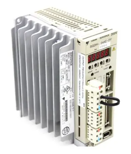
 Yaskawa SGDH-04AE-OY Servo Driver 400W 200V
 -
 OMRON CJ1H-CPU66H V4.0 PLC CPU
 -
 OMRON R7M-A10030-BS1 Servo Motor 200W 100V
 -
 OMRON FQM1-MMA21 Motion Controller
 -
 Yaskawa SJDE-08APA Servo Amplifier
 -
 OMRON CQM1-AD041 Analog Input Unit
 -
 Siemens OCI55 Dialogue Module Landis
 -
 OMRON F350-C10E Image Processing Unit
 -
 OMRON NT10S-SF121 HMI Terminal
 -
 SIEMENS 3RB1262-0LB31 Overload Relay
 -
 OMRON YASKAWA SGDS-02A12A Servo Drive
 -
 TE.CO TFX 4G 1.5 Grey Cable ST 500m
 -
 FANUC A16B-3200-0362 PCB Control Board
 -
OMRON CQM1-ARM21 Analog Output Unit
-
 Allen-Bradley 1788-EN2DN Ethernet DeviceNet Gateway
 -
 Siemens 3VL9440-7EE40 3VL4740-2AA46-0AA0 Circuit Breaker
 -
 OMRON CJ1W-AD041-V1 Analog Input Unit
 -
 OMRON CQM1-AD041 CQM1-IPS02 Analog Input Power Supply
 -
 Texas Instruments System 505 PLC 525-110 525-1102
 -
 OMRON CQM1-AD042 Analog Input Unit
 -
 Yaskawa SGDH-04AE-OY Servo Driver 200V 400W
 -
 CTI 2512 75W Power Supply for CTI 2500
 -
 Omron F300-B5 Image Processing Unit
 -
 Mitsubishi 15050-PR01A PLC Board
 -
 Omron CQM1-TC101 Temperature Controller
 -
 SCE M68-2000 2 Axis Motion Controller HW 2.3/B
 -
 Omron 3Z4SP-C22 Visual Positioning Sensor
 -
 Omron 3G3SV-BB007-E 0.75kW VFD
 -
 CML 6622 IRD Entek AW10528 Vibration Monitor
 -
 Omron CP1L-EL20DR-D PLC CPU
 -
 TE.CO TFX 4G 1.5 Grey Cable 500m
 -
 Mitsubishi Electric 3BK23057 Circuit Board Module
 -
 OMRON FQM1-MMP21 Motion Control Module
 -
 OMRON CP1E-E40SDR-A Micro PLC CPU Unit
 -
 KEBA CU201 PLC Control Unit
 -
 OMRON F150-C10E-2 Vision Sensor Controller
 -
 YASKAWA SGDH-04AE-OY Sigma-II Servo Driver
 -
 OMRON CS1H-CPU65-V1 PLC Central Processing Unit
 -
 OMRON NB7W-TX01B Interactive Display HMI
 -
 OMRON C500-TU002E Programmable Logic Controller Timer Unit
 -
 OMRON C200HW-PRT21 PROFIBUS DP Slave Unit
 -
 ExcelTech MX-5-S-I-6-4 Static Transfer Switch
 -
 Allen-Bradley 100-B300ND3 Contactor 304A 600V
 -
 Pasaban MTC-3052 Fast I/O PLC Card
 -
 OMRON CQM1-TC101 Temperature Control Unit
 -
 OMRON 3G3SV-BB007-E VFD 0.75kW 220V
 -
 OMRON CQM1H-MAB42 PLC Module
 -
 OMRON R88M-K75030T-S2 Servo Motor
 -
 Yaskawa SGMAH-03DAAA61 Servo Motor 200V 300W
 -
 OMRON F300-P Power Supply Unit
 -
 Land System 4 M1 Thermometer 65071800C-L35-A50
 -
 Yamatake MAH10-ME0100 ME-NET Module
 -
 Siemens Simatic 505 16 Slot PLC Rack
 -
 Yaskawa SGDH-02AE-OY Servo Driver 200W
 -
 SCE M68-2000 2-Axis Motion Controller
 -
 Zenith Controls K-1201 Transfer Switch Controller
 -
 Yaskawa SGDH-02AE-OY 200W Servo Driver
 -
 Yaskawa SGMAH-02AAA61D-0Y 200W Servo Motor
 -
 Schneider TSX P573634M Modicon Premium CPU
 -
 Siemens 6FX5002-5DN31-1DA0 Power Cable
 -
 Omron CJ1G-CPU43H CPU Unit 30K Steps
 -
 OMRON C28P-EDR-D PLC Unit
 -
 SIEMENS S7-300 PLC System
 -
 Schneider TP400-PLC-1411 Board
 -
 Siemens 6FC5203-0AF00-0AA3 Panel
 -
 ALLEN BRADLEY 1754-L28BBB GuardPLC
 -
 Omron E6C3-AG5B-C Encoder
 -
 SCE M68-2000/5 CNC Controller
 -
 SCHNEIDER TM2ALM3LT Module
 -
 OMRON C200H-OV001 Voice Module
 -
 OMRON R88M-H30030 Servo Motor
 -
 Bosch RD500 Indramat Servo Drive RD51.2-4B
 -
 Siemens 6SE7090-0XX84-0AH2 T300 Module
 -
 Omron GRT1-TS2P SmartSlice Thermocouple Input
 -
 Xaar XP55500016 XUSB Drive Electronics
 -
 Siemens 6SL3210-1SE21-8UA0 PM340 Power Module
 -
 Mitsubishi GT2708-VTBA Touch Display 8.4 Inch
 -
 Pasaban Fast I/O MTC-3052 PLC Card
 -
 ABB ACS355-01U-02A4-2 VFD 0.37kW
 -
 Yamatake MAH20-PC2100 Processor Module
 -
 Allen Bradley 1774-P1 PLC Power Supply
 -
 Yaskawa SGDH-04AE-OY 400W Servo Driver
 -
 Omron CPH-X40DT1-D PLC CPU Unit
 -
 Pilz PNOZ mm0.2p Safety PLC Mini 772002
 -
 Siemens 6SL3555-OPR01-0AA0 Sinamics G110M Panel
 -
 Sanyo PLC-XTC50L LCD Projector
 -
 SCE M68-2000 2-Axis Motion Controller
 -
 Omron CS1W-CT021 High-Speed Counter Unit