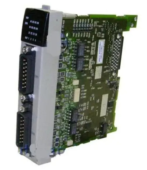
MVME51005E Single Board Computer Installation and Use
Installation and Use
If an ESD station is not available, you can avoid damage resulting from ESD by wearing an antistatic wrist strap (available locally) that is attached to an active electrical ground.Note A system chassis may not be a suitable grounding source if it is unplugged.
Hardware and Firmware InitializationThe debugger performs the hardware and firmware initialization process. This process occurs each time the MVME5100 is reset or powered up. The steps listed below are a high-level outline; be aware that not all of the detailed steps are listed.1.Sets MPU.MSR to known value.2.Invalidates the MP
U's data/instruction caches.3.Clears all segment registers of the MPU.4.Clears all block address translation registers of the MPU.5.Initializes the MPU-bus-to-PCI-bus bridge device.6.Initializes the PCI-bus-to-ISA-bus bridge device.7.Calculates the external bus clock speed of the MPU.8.Delays for 750 milliseconds.9.Determines the CPU base board type.10.Sizes the local read/write memory (that is, DR AM).11.Initializes the read/write memory controller. Sets base address of memory to 0x00000000.12.Retrieves the speed of read/write memory.13.Initializes the read/write memory controller with the speed of read/write memory.14.Retrieves the speed of read only memory (thatis,Flash).15.Initializes the read only memory controller with the speed of read only memory.16.Enables the MPU's instruction cache. 17.Copies the MPU's exception
vector table from 0xFFF00000 to 0x00000000.18.Verifies MPU type.19.Enables the superscalar feature of the MPU (superscalar processor boards only).20.Verifies the extern
al bus clock speed of the MPU.21.Determines the debugger's console/host ports and initializes the PC16550A.22.Displays the debugger's copyright message.23.Displays
any hardware initialization errors thatmay have occurred.24.Checksums the debugger object and displays a warning message if the checksum failed to verify.
25.Displays the amount of local read/write memory found.
26.Verifies the configuration data that is resident in NVRAM and displays a warning message if the verification failed.
27.Calculates and displays the MPU clock speed, verifies that the MPU clock speed matches the configuration data, and displays a warning message if the verificationfails.
28.Displays the BUS clock speed, verifies that the BUS clock speed matches the configuration data,and displays a warning message if the verification fails.29.Probes PCI bus for supported network devices.30.Probes PCI bus for supported mass storage devices.31.Initializes the memory/IO addresses for the supported PCI bus devices.32.Executes Self-Test, if so configured. (Default is no Self-Test).33.Extinguishes the board fail LED, if Self-Test passed and outputs any warning messages.
34.Executes boot program, if so configured. (Default is no boot.)35.Executes the debugger monitor (that is, issues the PPC6-Bug> prompt).
System Memory Controller and PCI Host Bridge:
The on-board Hawk ASIC provides the bridge function between the processor’s bus and the PCI bus. It provides 32-bit addressing and 64-bit data; however, 64-bit addressing (dual address cycle)is not supported. The ASIC also supports various processor external bus frequencies up to100 MHz.
There are four programmable map decoders for each direction to provide flexible address mappings between the processor and the PCI bus. The ASIC also provides an Multi-Processor Interrupt Controller (MPIC) to handle various interrupt sources. They are: four MPIC timer interrupts, interrupts from all PCI devices and two software interrupts.
Memory :
The following subsections describe various memory capabilities on the MVME5100 including Flash memory and ECC SDRAM memory.
Flash Memory:
The MVME5100 contains two banks of Flash memory. Bank B consists of two 32-pin devices which can be populated with 1MB of Flash memory (only 8-bit writes are supported for this bank). Refer to the application note following for more write-protect information on this product.
Bank A has 4 16-bit Smart Voltage FLASH SMT devices. With 32Mbit flash devices, the flash memory size is 16MB. Note that only 32-bit writes are supported for this bank of flash memory.Application Note: For Am29DL322C or Am29DL323C, 32Megabit (4M x 8-Bit/2M x 16-bit) CMOS 3.0 Volt-only Flash Memory.TheWrite Protect function provides a hardware method of protecting certain boot sectors. If the system asserts V IL (low signal) on the WP#/ACC pin, the device disables the program and erase capability, independently of whether those sectors were protected or unprotected using the method described in the Sector/Sector Block Protection and Unprotection of the AMD datasheet. The two outermost 8Kbyte boot sectors are the two sectors containing the lowest addresses in a bottom-boot-configured device, or the two sectors containing the highest addresses in a top-boot-configured device.
The aforementioned implemented device (at the time of this printing is the only qualified Flash device used on this product) is a top-boot device, and as such, the write protected area is in the upper 16KB of each device. Since it uses 4 devices for the soldered Flash bank, the write protected region corresponds to the upper 64KB of the soldered Flash memory map. Thus the address range of $F4FF 0000 to F4FF FFFF is the write protected region when the J16 header is jumpered across pins 2 and 3.If PPCBug tries to write to those write-protected address areas whenpins 2-3 on J16 are set, the command will simply not finish (i.e., erase sector function stops at $F4FF 0000).
- ABB
- General Electric
- EMERSON
- Honeywell
- HIMA
- ALSTOM
- Rolls-Royce
- MOTOROLA
- Rockwell
- Siemens
- Woodward
- YOKOGAWA
- FOXBORO
- KOLLMORGEN
- MOOG
- KB
- YAMAHA
- BENDER
- TEKTRONIX
- Westinghouse
- AMAT
- AB
- XYCOM
- Yaskawa
- B&R
- Schneider
- Kongsberg
- NI
- WATLOW
- ProSoft
- SEW
- ADVANCED
- Reliance
- TRICONEX
- METSO
- MAN
- Advantest
- STUDER
- KONGSBERG
- DANAHER MOTION
- Bently
- Galil
- EATON
- MOLEX
- DEIF
- B&W
- ZYGO
- Aerotech
- DANFOSS
- Beijer
- Moxa
- Rexroth
- Johnson
- WAGO
- TOSHIBA
- BMCM
- SMC
- HITACHI
- HIRSCHMANN
- Application field
- XP POWER
- CTI
- TRICON
- STOBER
- Thinklogical
- Horner Automation
- Meggitt
- Fanuc
- Baldor
- SHINKAWA
- Other Brands
- UniOP
- KUKA
- Iba


