
ABB IGCT Technology: A Revolutionary Breakthrough in High Voltage Inverters
To solve this dilemma, ABB Switzerland is exploring a new research and development path aimed at integrating the high-power advantages of IGBT with the core strengths of GTO, ultimately developing GCT (Gate Commutated Thyristor) and further developing it into IGCT, becoming an ideal alternative technology for GTO.
ABB IGCT Technology: A Revolutionary Breakthrough in High Voltage Inverters
Background and original intention of technology research and development
The development of power semiconductors has always been aimed at pursuing the "ideal switch", which requires the characteristics of low pass state and commutation loss, high commutation frequency, and simple driving circuit. In the low-voltage field, the technological iteration from transistors and Darlington transistors to IGBT (Insulated Gate Bipolar Transistor) has achieved significant results. However, in the medium to high voltage field, the long-term dependence on GTO (Gate Turn Off Thyristor) poses problems such as complex control and limited performance.
To solve this dilemma, ABB Switzerland is exploring a new research and development path aimed at integrating the high-power advantages of IGBT with the core strengths of GTO, ultimately developing GCT (Gate Commutated Thyristor) and further developing it into IGCT, becoming an ideal alternative technology for GTO.
Principles and Breakthroughs of IGCT Core Technology
(1) Core improvement of GCT: solving GTO control problems
GTO has serious control issues and requires an unstable transition zone where both anode voltage and cathode current act simultaneously during shutdown, relying on buffer circuits for support. GCT breaks through this limitation through "hard drive" technology:
The rate of change of gate current reaches µ
(far exceeding GTO's 50 A/µ s), it can switch the current from the cathode to the gate before there is a significant change in the charge distribution between the gate and anode.
Directly switch the device from thyristor mode to transistor mode, with stable and fast turn off process, no need for buffer circuit, and performance close to IGBT.
(2) The Four Key Development Steps of IGCT Converter
Low inductance drive design
To avoid the GCT entering the unstable working zone, the cathode current needs to be turned off within 1 µ s, and the leakage inductance of the gate circuit corresponding to the 3kA GCT should be ≤ 6nH (only 1/50 of the conventional value of GTO).
Low inductance is achieved through a multi-layer connection between the coaxial device connection structure and the driving power output, while using a gate voltage of -20V to balance reliability and cost-effectiveness.
Optimize silicon wafer technology
Hard drive technology allows GCT silicon wafers to be designed thinner without compromising on switch characteristics, combined with plasma engineering technology, significantly reducing losses (compared to GTO of the same specification, the commutation loss is similar but the on state loss is lower).
High integration and linear scaling of current
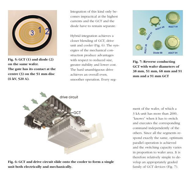
Integration is divided into two levels: one is single-chip integration (integrating anti parallel diodes and GCTs on the same silicon wafer to reduce diode stacking and high current connections); The second is hybrid integration (integrating GCT, driving unit, and cooler to reduce volume, improve stability, and lower costs).
Each unit of the silicon wafer (3kA devices containing over 2000 units) synchronously responds to switch instructions, achieving optimal parallel operation. The current capacity is linearly related to the silicon wafer area, making it easy to develop multi specification GCT series (such as devices with silicon wafer diameters of 38mm, 51mm, 68mm, and 91mm).
Simplify circuit complexity
No buffering capacitors, diodes, and resistors are required for GTO converters, only the current rise rate when GCT is turned on needs to be limited (as high-voltage silicon diodes are slower than low-voltage IGBT diodes).
By adopting a new high current circuit, all phases of the inverter can be connected to the same DC bus, which is comparable in cost to conventional IGBT converters.
(3) Modular design and high-voltage adaptation
Modular component system: In response to the diverse application requirements and small batch size of high-power converters, IGCT adopts modular design, which can cover a power range of 250kW to 100MW through unit series connection and adapt to different scenarios.
Pressure contact technology: Traditional module technology is difficult to handle high voltage and high current. IGCT adopts an improved pressure contact technology, which integrates the driving unit, power semiconductor, and cooler into a single functional unit. It replaces expensive chip parallel arrays with optimized silicon wafers in standard packaging, simplifies manufacturing, reduces costs, and is easy to maintain.
Performance advantages and application cases of IGCT converters
(1) Core performance advantages
Category specific advantages
Component characteristics include high rated voltage, low turn-on and commutation losses, high commutation frequency (intermittent up to 7kHz, average 500Hz for three-point converters, equivalent two-point 2kHz), high silicon wafer utilization, uniform current distribution, linear correlation between current capacity and silicon wafer area, and easy modeling
Circuit design includes a three-phase shared DC bus, a central dI/dt limiter with integrated clamping, simple intermediate circuit connection, safety and reliability under extreme working conditions, and a simple driving circuit (directly coupled with switch signals, no dV/dt or dI/dt regulation circuit required, dual line low-power power supply)
- OMRON
- ABB
- General Electric
- EMERSON
- Honeywell
- HIMA
- ALSTOM
- Rolls-Royce
- MOTOROLA
- Rockwell
- Siemens
- Woodward
- YOKOGAWA
- FOXBORO
- KOLLMORGEN
- MOOG
- KB
- YAMAHA
- BENDER
- TEKTRONIX
- Westinghouse
- AMAT
- AB
- XYCOM
- Yaskawa
- B&R
- Schneider
- KONGSBERG
- NI
- WATLOW
- ProSoft
- SEW
- ADVANCED
- Reliance
- TRICONEX
- METSO
- MAN
- Advantest
- STUDER
- DANAHER MOTION
- Bently
- Galil
- EATON
- MOLEX
- DEIF
- B&W
- ZYGO
- Aerotech
- DANFOSS
- Beijer
- Moxa
- Rexroth
- Johnson
- WAGO
- TOSHIBA
- BMCM
- SMC
- HITACHI
- HIRSCHMANN
- Application field
- XP POWER
- CTI
- TRICON
- STOBER
- Thinklogical
- Horner Automation
- Meggitt
- Fanuc
- Baldor
- SHINKAWA
- Other Brands
- UniOP
- KUKA
- Iba
- Beckhoff
-
 FUJI UG430H-TS1 HMI Touch Panel
 -
 Westronics CB100188-01 Rev F Board
 -
 Siemens 7MH4900-3AA01 Weighing Module
 -
 Gilbert & Nash Tracker 2000 Control Cabinet
 -
 OMRON CJ1M-CPU22 CPU Unit
 -
 OMRON F3SJ-E0625P25 Light Curtain
 -
 Siemens 3VA2340-5HL32-0AA0 Breaker
 -
 Mitsubishi Melsec A61P A2NCPU PLC System
 -
 Aeco 158-02 DSP-02 PCB Card
 -
 FUJI NP1PS-32R CPU Module
 -
 Siemens 6SL3040-1MA01-0AA0 Control Unit CU320-2 PN
 -
 Fuji RYE.75D PLC Driver AC Drive
 -
 Electro Cam PS-6144-24-P16M09-L-MB Programmable Limit Switch
 -
 Siemens C98043-A7001-L2-4 CUD1 Control Board
 -
 Pilz 312070 PSSu H PLC1 FS SN SD Safety Module
 -
 Siemens Plc42q4200atsn Circuit Breaker Fuse Box
 -
 GE Fanuc IC695ALG708-AB Analog Output Module Rx3i
 -
 Siemens 6SE7036-5GK84-1JC2 IGD8 Gate Driver Board
 -
 Charmilles 813078 852029 PLC PCB Robocut 2 CNC EDM
 -
 Siemens 6SL3130-1TE24-0AA0 Smart Line Module
 -
 Pasaban MTC3001-DC Drive Control PLC Module
 -
 Modicon AS-P890-000 Remote I/O Processor Power Supply
 -
 Siemens PXC100-PE96.A PXC Modular Controller
 -
 TOYO KEIKI P:CARD5 AVH-R YH-212 Industrial Control Card
 -
 Omron NS5-SQ00B-V2 HMI Touch Screen 5.7 Inch
 -
 Sciemetric SigPOD 1202-0H00 Data Acquisition Module
 -
 GE Fanuc IC693CPU331W CPU Module Series 90-30
 -
 Square D 8903SVO11V02 Lighting Contactor 200A
 -
 Beckhoff C9900-P224 Power Supply Unit 24V 10A
 -
 HSD PE323 PLC I/O Module
 -
 Pillar AB6406-11A Power Control Board
 -
 GE Fanuc IC693CPU331W CPU Module
 -
 FANUC A61L-0001-0072 LCD Monitor
 -
 AB 20D-D-011-A-0-EYNANANE Drive
 -
 AB 1785-L20B PLC-5/20 Processor
 -
 Siemens SIREC P/PA Recorder 7ND3021
 -
 Siemens D2E160-AH01-17 Fan Blower
 -
 Eaton 101073735-001 LEG Module
 -
 AB 1404-M605B-ENT Powermonitor 3000
 -
 OMRON CJ1W-MAD42 Analog I/O
 -
 Omron CJ1M-CPU13 V3.0 PLC CPU Module
 -
 Pe323 HSD PLC Module Industrial Controller
 -
 Pasaban MTC3001-DC Drive Control PLC Module
 -
 Mitsubishi R02CPU PLC Module MELSEC iQ-R
 -
 B&R X20DC2395 Digital Output Module 32 Ch
 -
 Hoffman A30N24ALP Enclosure with PLC Addons
 -
 Rieter PLC with RMC 24/5V 10 RMC188-1 RMC RIO-1
 -
 Allen-Bradley 1790D-TN4V0 CompactBlock LDX Base Block 4 AI
 -
 National Instruments NI 9242 Analog Input Module 4-Channel
 -
 ABB AO820 3BSE008546R1 Analog Output Module
 -
 Moeller XVC-101-C192K-K82 PLC
 -
 AB 440F-C4000P MatGuard Controller
 -
 AB 1692-ZRCLSS Protection Module
 -
 Schneider S48896 PLC Module
 -
 FANUC A02B-0303-C205 I/O Module
 -
 AB 1785-LT4 PLC-5/10 Processor
 -
 AB 1746-NO8V SLC 500 Analog Output
 -
 OMRON CQM1-TC001 Temperature Unit
 -
 OMRON R7M-A20030-S1 Servo Motor
 -
 Toshiba ST1500GXH24 IEGT Module
 -
 Infineon PEF22822F V2.2 IC ISDN Controller
 -
 Allen-Bradley 440R-D22S2 Guardmaster Safety Relay GSR
 -
 Allen-Bradley 1771-IJ PLC Encoder Counter Module TTL
 -
 Texa Industrie EGO16GT1B Wall Frame Air Conditioner PLC
 -
 Schleicher Master CPU UCH 2 High Speed PLC
 -
 Siemens 6FC5371-0AA10-0AA1 NCU 710.2 CNC Controller
 -
 Schneider TM221C40R Modicon M221 PLC 40 I/O
 -
 Mitsubishi FX3U-128MR/ES PLC Controller 128 I/O
 -
 Pepperl Fuchs KFD0-RSH-1.4S.PS2 Relay Module 24VDC
 -
 Schneider XBTGT2110 HMI Touch Panel 10.4 Inch
 -
 APPLIED MATERIALS 0100-03267 - CH FACILITY INTERFACE PRODUCER SE PCB ASSY
 -
 INFICON 921-250-G1 - FFS232 Fabguard Interface AMAT Endura
 -
LEYBOLD 0730-01046 - TRUBOTRONIK CONV FREQ NT341 MC/MCT 208V CONTROLLER
-
 APPLIED MATERIALS 0010-57168 - SENSOR BOX ASM 300MM 35013
 -
 APPLIED MATERIALS 0226-31128 - ASSY VERSION 4 SIGNAL LAMP PCB
 -
 SBS 0090-01220 - PCB CPU BOARD FOR 128-30000
 -
 AMAT - - ANODE BULK COPPER PELLETS FG01PLT
 -
 APPLIED MATERIALS 0041-26804 - SHUTTER DOOR DRIVE ASSY 0040-76764 32032
 -
 APPLIED MATERIALS 0040-75150 - FILLER CHAMBER 1 APF PRODUCER SE
 -
 AMAT 0190-33295 - GATE COMPL
 -
 Applied Materials 0010-09341 - Wafer lift precision 5000 AMAT
 -
 APPLIED MATERIALS 0190-32096 - VARIAN CONTROLLER ASSY E15006160 E11388030
 -
 AMAT 0090-00590 - ELECT ASSY 750W SERVO MOTOR
 -
APPLIED MATERIALS 101294-01 - 550W Power Supply
-
 APPLIED MATERIALS 0150-14869 - CABLE AMAT LOT OF 16
 -
Applied Materials 0200-09830 - ESC Electrostatic Chuck Pedestal Ring
-
 APPLIED MATERIALS 0021-89500 - BRKT SNSR UPPER FRAME HTF 16132
 -
 Applied Materials 0200-10555 - Quartz Baseplate with Baffle 0200-00715
 -
 APPLIED MATERIALS 0240-75851 - KIT 11.3" SOURCE INSTALL
 -
 Applied Materials 0040-22023 - Adapter 13" W/B Source
 -
 Applied Materials 0010-09416 - P5000 Etch Std 3 kW 13.56 MHz Match
 -
AMAT - - System Electronics Interface Board assy
-
 AMAT 0090-00836 - MOTOR ASSY ROTATION 300MM
 -
 APPLIED MATERIALS 0140-12304 - HARNESS ASSY MF REMOTE SIGNALS PRODUCE 13041
 -
 Applied Materials 9090-01168ITL - ESC Chuck Power Supply PX32J
 -
 APPLIED MATERIALS 0020-24099 - insulator
 -
 APPLIED MATERIALS 0190-09764 - ZERO FIRING VARIABLE TIME BASE SCR POWER
 -
APPLIED MATERIALS 0190-29887 - VERITY FL2006 FLASH LAMP 1007454 32453
-
 APPLIED MATERIALS 0010-09348 - ASSY UNIVERSAL THROTTLE VALVE
 -
 APPLIED MATERIALS 0190-61486 - PRE-ALIGNER
 -
 APPLIED MATERIALS 0100-20000 - PCB ASSY 64 CHANNEL MUX 34246
 -
 Applied Materials 0090-07393 - RF Filter unit
 -
AMAT 0040-89462 - FLANGE 6 PORT 300MM TITAN CONTOUR
-
 APPLIED MATERIALS 0021-01421 - CHAMBER UPPER A-COAT M-DPS 32824
 -
Applied Materials 0242-37433 - EMPAK 200mm Cassette Handler Retrofit Kit
-
 APPLIED MATERIALS 0190-49999 - LINEAR ACTUATOR ASSY 32429
 -
 APPLIED MATERIALS 0020-63694 - COVER 300MM TITAN CONTOUR
 -
 APPLIED MATERIALS 0150-11135 - P3 MULTIZONE CTRL UNIT REV 002 11362100 1917
 -
 APPLIED MATERIALS 0240-01698 - KIT BAFFLE CLEAN PORT ULTIMA HDP-CVD
 -
 APPLIED MATERIALS 0040-03799 - MOUNTING PLATE CR SWILL
 -
 Applied Materials 0190-23562 - Newport 40000 Servo Positioning Controller
 -
 APPLIED MATERIALS 0090-08798 - ASSY EPM OVERSAMPLE INPUT CONTROLLER 28223
 -
 APPLIED MATERIALS 0040-32052 - WELDMENT BELLOW CATHODE DPSGECO 19601
 -
 APPLIED MATERIALS 0190-35712 - ASSY P-CHUCK 200MM CIP 99 0010-38437 35695
 -
 APPLIED MATERIALS 0021-39748 - BLOCKER PERF SILANE NITRIDE550 14762
 -
 APPLIED MATERIALS 3870-02323 - NOR-CAL VALVE PNEU INLINE 1" NW25 VIT-SEAL 12790
 -
 APPLIED MATERIALS 01-81911-00 - 8100 N ION TC CONTROLLER
 -
 APPLIED MATERIALS 0010-19137 - DEGAS LIFT & MOTOR ASSY 38924
 -
 APPLIED MATERIALS 0010-09978 - LAMP MODULE ASSY
 -
 APPLIED MATERIALS 0190-02362 - PCB ASSY MAINFRAME INTLK 1 RELAYS 32352
 -
AMAT 0010-07017 - PCB ASSEMBLY LOWER PNEUMATIC BD
-
 APPLIED MATERIALS 0010-75226 - ASSY THROTTLE VALVE 200MM ETCH DOWN STREAM 38918
 -
 APPLIED MATERIALS 0010-70345 - 0042-01927 Component
 -
 APPLIED MATERIALS 0010-07586 - ASSY HUB RADIANCE CHAMBER 33456
 -
 Applied Materials 0020-33882 - R2 Standard Cathode Insulating Washer
 -
 AMAT - - Pneumatic Door Assembly Desica Cleaner
 -
 APPLIED MATERIALS 3250-00041 - CNTNR DEIONIZER TANK SST HI TEMP W/RESIN
 -
APPLIED MATERIALS 0190-E1370 - TWIN DETECTOR ASSY 38070


